

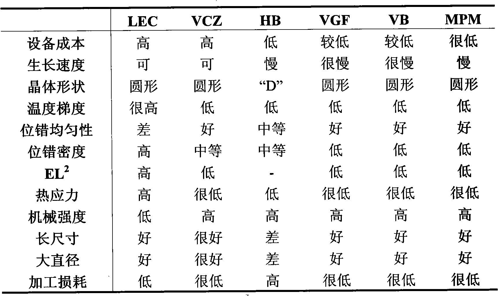
Improved Bridgman-Stockbarger method for compound semiconductor GaAs single crystal
A technology of crucible drop method and growth method, which is applied in the directions of single crystal growth, single crystal growth, crystal growth, etc., and can solve the problems of low production efficiency and the like
- Summary
- Abstract
- Description
- Claims
- Application Information
AI Technical Summary
Problems solved by technology
Method used
Image

Examples
Embodiment 1
[0011] Embodiment 1: Improved crucible drop method growth method for compound semiconductor GaAs single crystal:
[0012] Descending furnace selection: the multi-station crucible descending furnace is used for the growth of compound semiconductor GaAs single crystal;
[0013] Raw material preparation: Using high-purity As and Ga raw materials, GaAs polycrystalline material is synthesized by chemical reaction under airtight conditions. According to the needs of the experiment, excessive As is deliberately added during the batching. The excess of Arsenic is generally controlled to be less than 1 mol%, while the Si, Zn or Te impurities doped in the polycrystalline raw material are not more than 1 mol%.
[0014] Growth preparation: select high-quality GaAs crystals, precisely orientate them with an X-ray directional instrument, cut and grind them into the required shape, clean them and put them into the seed well position of the PBN crucible, then fill them with polycrystalline ma...
example 1
[0019] Example 1: Put 4.0 kg of As-rich high-purity GaAs polycrystalline raw material into a PBN crucible with a diameter of 3 inches, and a seed crystal with a orientation and a diameter of 10 mm is placed on the bottom of the crucible in advance. Then put the crucible in the descending method crystal growth furnace, the temperature of the furnace is controlled at 1280°C, and the inoculation growth starts after the temperature is constant. The growth period is 5 days. After the growth is completed, anneal at 1000°C for 10 hours in a constant temperature zone, and slowly cool down to room temperature to obtain GaAs crystals with bright and non-wetting surfaces.
example 2
[0020] Example 2: Put 16.0 kg of As-rich high-purity GaAs polycrystalline raw material into four PBN crucibles with a diameter of 3 inches, respectively, and placed -oriented seed crystals with a diameter of 10 mm at the bottom of the crucibles in advance. Then put the 4 crucibles in a multi-station descending method crystal growth furnace. The temperature of the furnace is controlled at 1280° C., and the inoculation growth starts after the temperature is constant. The growth cycle is 5 days. After the growth, anneal at 1000°C for 10 hours in a constant temperature zone, and slowly cool down to room temperature. Four GaAs crystals of the same length with bright surfaces and no wetting can be obtained.
PUM
 Abstract
Description
Claims
Application Information