

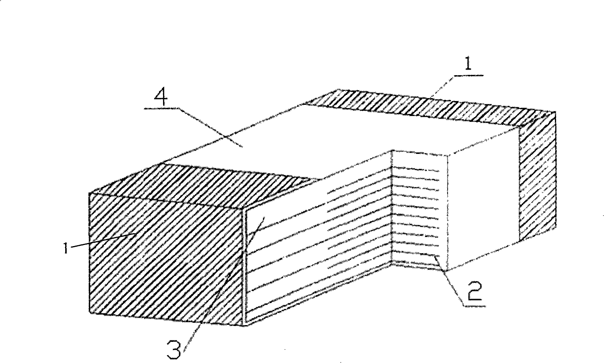
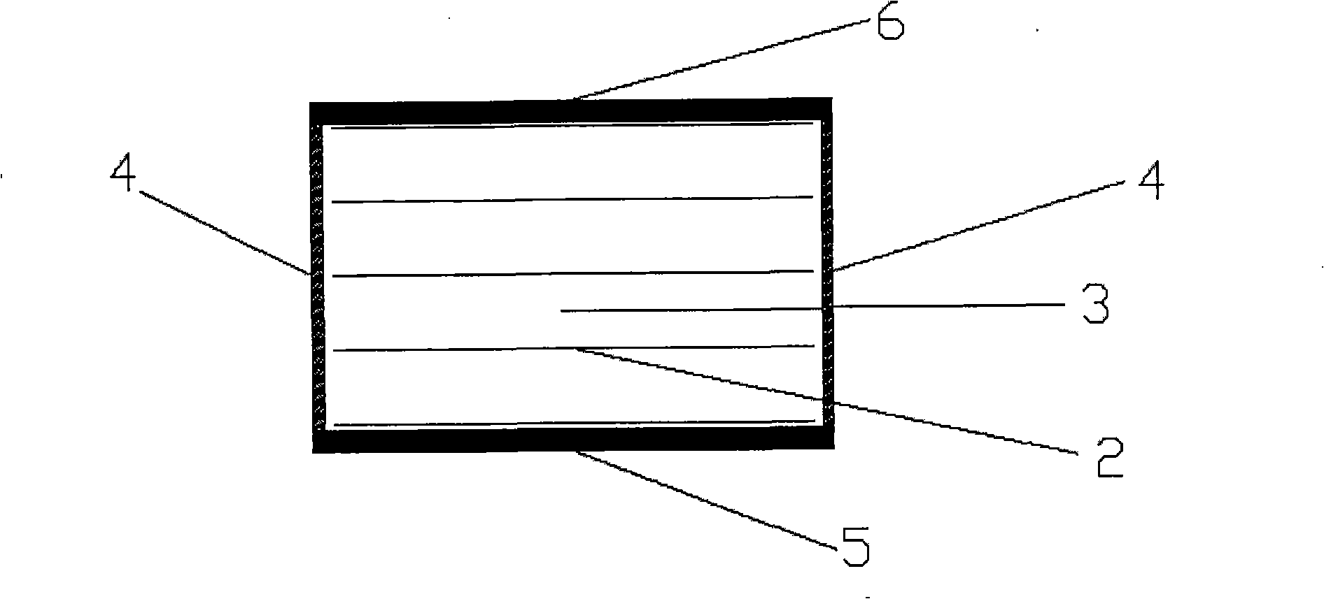
Stacking slice type piezoresistor and manufacturing method thereof
A technology of varistors and varistors, which is applied in the fields of varistor cores, resistance manufacturing, varistors, etc., can solve the problems that the products are not easy to electroplate nickel, tin treatment, low pass rate, high production cost, etc. Achieve the effect of improving welding reliability, increasing pass rate, and solving performance deterioration
- Summary
- Abstract
- Description
- Claims
- Application Information
AI Technical Summary
Problems solved by technology
Method used
Image

Examples
Embodiment 1
[0052] The manufacturing method of the multilayer chip varistor provided in this embodiment includes the following steps:
[0053] (1) Powder preparation: use ceramic protective film materials and varistor film materials to manufacture corresponding powders respectively.
[0054] The piezoresistive film powder is ground with piezoresistive film material and uniformly mixed for 30 hours to a particle size of 1.0 μm, dried at 150°C, and sieved with 80 meshes. The components of the materials used and their contents (weight) are:
[0056] Bismuth oxide Bi 2 o 3 3.5%
[0057] Antimony oxide Sb 2 o 3 5%
[0058] Cobalt oxide Co 3 o 4 2%
[0059] Manganese Carbonate MnCO 3 0.5%
[0060] Chromium oxide Cr 2 o 3 1%
[0061] Nickel oxide Ni 2 o 3 1%
[0062] Aluminum nitrate Al(NO 3 ) 3 9H 2 O 0.01%
[0063] Silver nitrate AgNO 3 0.02%
[0064] boric aci...
Embodiment 2
[0095] The manufacturing method of the multilayer chip varistor according to the embodiment of the present invention includes the following steps:
[0096] (1) Powder preparation: use ceramic protective film materials and varistor film materials to manufacture corresponding powders respectively.
[0097] The piezoresistive film powder is ground with piezoresistive film material and uniformly mixed for 30 hours to a particle size of 1.0 μm, dried at 150°C, and sieved with 80 meshes. The components of the materials used and their contents (weight) are:
[0099] Bismuth oxide Bi 2 o 3 5%
[0100] Antimony oxide Sb 2 o 3 3.7%
[0101] Cobalt oxide Co 3 o 4 1.6%
[0102] Manganese Carbonate MnCO 3 1.5%
[0103] Chromium oxide Cr 2 o 3 0.8%
[0104] Nickel oxide Ni 2 o 3 1%
[0105] Aluminum nitrate Al(NO 3 ) 3 9H 2 O 0.01%
[0106] Silver nitrate AgNO ...
PUM
| Property | Measurement | Unit |
|---|---|---|
| Thickness | aaaaa | aaaaa |
| Thickness | aaaaa | aaaaa |
Abstract
Description
Claims
Application Information