
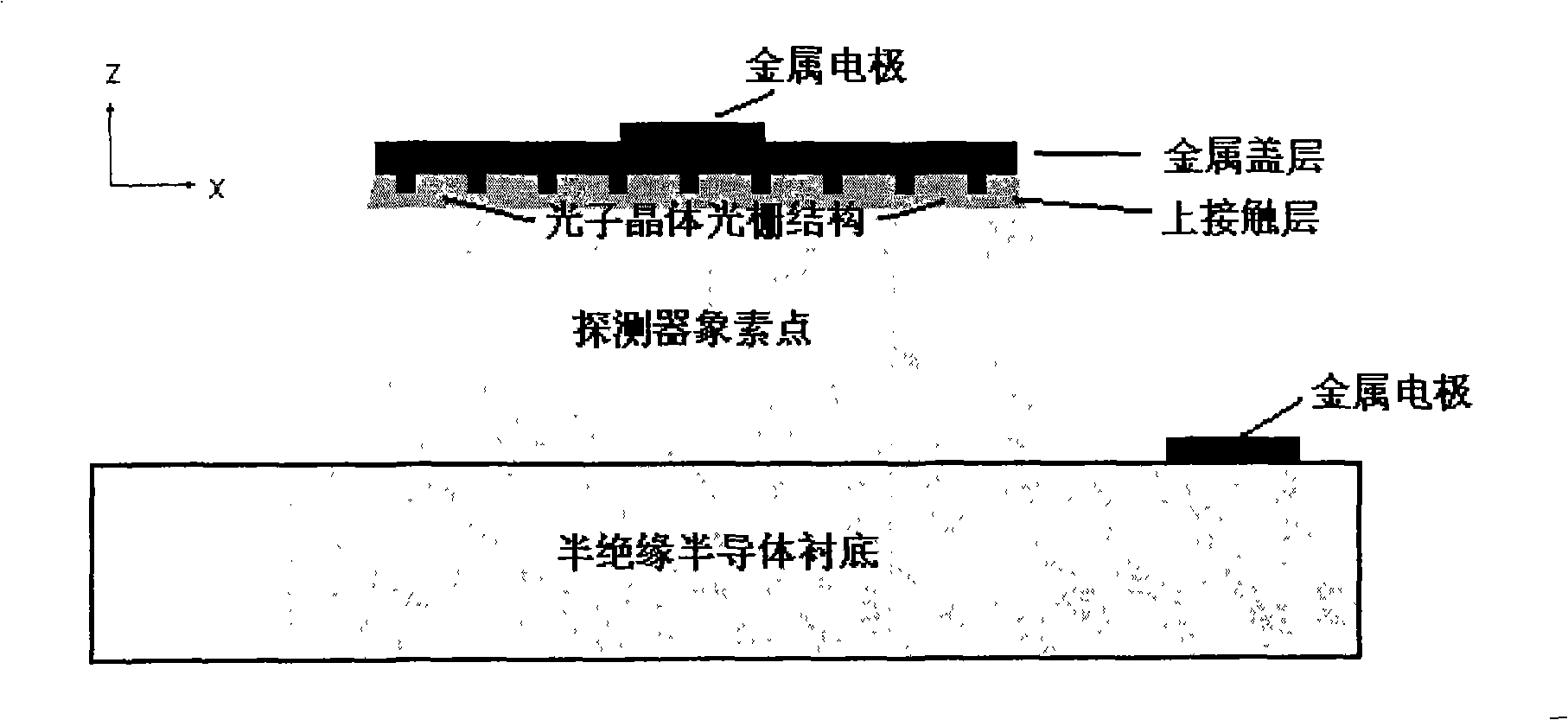
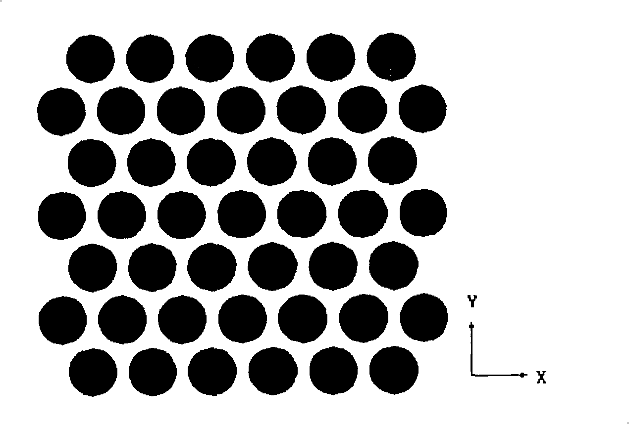
Photon crystal grating on the top of a dual-color infrared quantum well detector

A photonic crystal, two-dimensional photonic crystal technology, applied in diffraction gratings, optics, instruments, etc., to achieve the effects of easy preparation, high coupling efficiency, and efficient polarization modulation

Active Publication Date: 2009-01-21
INST OF SEMICONDUCTORS - CHINESE ACAD OF SCI
View PDF0 Cites 11 Cited by
  • Summary
  • Abstract
  • Description
  • Claims
  • Application Information

AI Technical Summary

Problems solved by technology

[0011] In view of this, the main purpose of the present invention is to provide a photonic crystal grating structure at the top of the two-color infrared quantum well focal plane detector, to solve the design and manufacture problems of the top grating of the two-color infrared quantum well focal plane detector, and to achieve simultaneous detection of two The purpose of higher coupling efficiency in a detected band

Method used


Image

  • Photon crystal grating on the top of a dual-color infrared quantum well detector
  • Photon crystal grating on the top of a dual-color infrared quantum well detector
  • Photon crystal grating on the top of a dual-color infrared quantum well detector

Examples


Embodiment 1

[0040] In this example, the working point of the two-color quantum well infrared detector is 5 μm in medium wave and 8 μm in long wave. In this example, a double-color pixel overlapping quantum well detector is used as the photoelectric conversion unit. The medium-wave absorption zone and the long-wave absorption zone adopt AlGaAs / GaAs quantum well structures with different Al components, and the vertical distance between the two absorption zones is d ′=1μm or so. According to Figure 4(a), we can see the normalized coupling efficiency of photonic crystal gratings with different periods under the condition of λ=5μm and λ=8μm. The left half of the figure corresponds to the coupling efficiency of λ=5μm, and the right half Corresponding to the coupling efficiency of λ=8μm, they have higher coupling efficiency around the period Λ=3μm. In the figure, d represents the distance between the horizontal section of the quantum well absorption zone and the bottom surface of the grating. When d...

Embodiment 2

[0044] In this example, the working points of the dual-color quantum well infrared detectors are all in the long wave 8μm / 12μm. It is only necessary to adjust the structural parameters to a circular hole triangular lattice photonic crystal structure with a period Λ = 4.6 μm, a duty ratio of r / Λ = 0.35, and a depth of h = 0.7 μm as the grating. Other parameters remain the same as in Example 1. The result can be changed, and the result is similar to that of Example 1. For details, please refer to Figure 4(b).


PUM


Abstract

The invention relates to the technical field of a semiconductor opto-electronic device, which discloses a photon crystal grating which is arranged on the top of a two-color infrared quantum well detector, wherein the photon crystal grating comprises a one-dimensional and a two-dimensional photon crystal structures and a metallic cover layer, wherein the two-dimensional photon crystal structure adopts a round hole or an elliptical hole which is etched on a semiconductor material on the top of the two-color semiconductor quantum well detector, and a material which the same with that of the metallic cover on the top is filled in the hole, and the metallic cover layer covers on the two-dimensional photon crystal structure. With the invention, the preparation technique of an infrared focal plane is simplified, and the coupling efficiency of two wave ranges is improved.

Description

Technical field [0001] The invention relates to the technical field of semiconductor optoelectronic devices, in particular to a photonic crystal grating on the top of a two-color infrared quantum well detector. Background technique [0002] Quantum well infrared detectors are key components of infrared technology, especially dual-color quantum well infrared detectors, which have become one of the focus of detector research in recent years. They integrate large-area, low-cost infrared focal plane staring systems and are widely used Military, meteorological, aerospace, medical and other technical fields. [0003] The principle of the quantum well infrared detector is to alternately grow semiconductor materials with different band gaps to form a quantum well structure, and use the sub-band transition of the quantum well to achieve photoelectric absorption conversion. According to the selection rule of quantum well subband transition, only light waves whose electric field direction i...

Claims


Application Information

Patent Timeline
IPC IPC(8): H01L31/0232G02F1/35G02B5/18
Inventor 郑婉华王科任刚杜晓宇邢名欣陈良惠
Owner INST OF SEMICONDUCTORS - CHINESE ACAD OF SCI
Learn More