Gap tunable triple thin-film solar cell and preparation thereof

A technology of solar cells and thin films, which is applied in the field of adjustable bandgap three-junction thin film solar cells and its production, to achieve the effects of reducing production costs, improving photoelectric conversion efficiency, and reducing reflection and transmission losses

Inactive Publication Date: 2009-03-11
SHANGHAI INST OF MICROSYSTEM & INFORMATION TECH CHINESE ACAD OF SCI
View PDF0 Cites 17 Cited by
  • Summary
  • Abstract
  • Description
  • Claims
  • Application Information

AI Technical Summary

Problems solved by technology

There are also few reports on the three-section structure. For example, the US Uni-solar company has introduced an amorphous silicon/amorphous silicon germanium

Method used


Image

  • Gap tunable triple thin-film solar cell and preparation thereof
  • Gap tunable triple thin-film solar cell and preparation thereof
  • Gap tunable triple thin-film solar cell and preparation thereof

Examples


Embodiment Construction

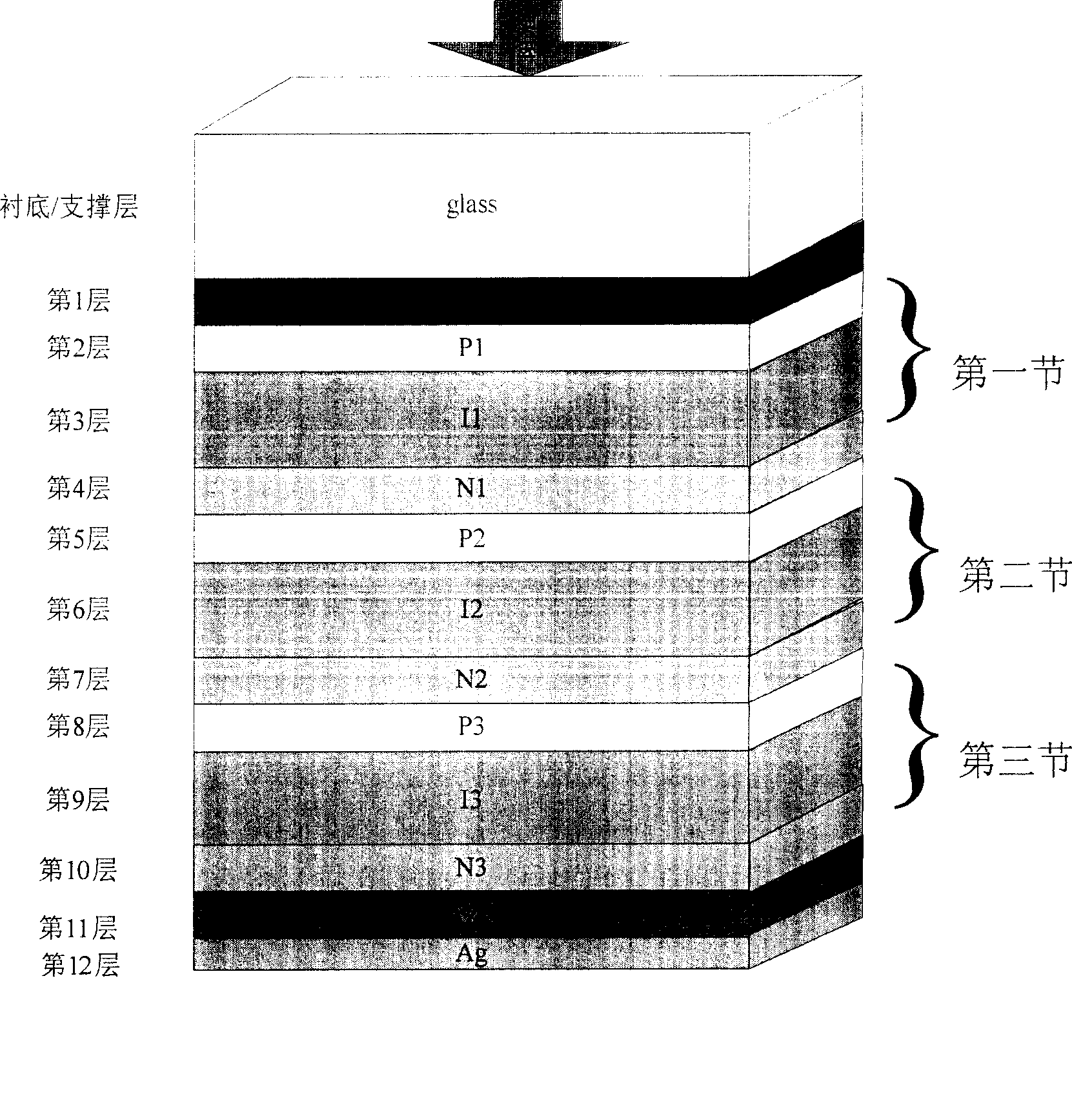
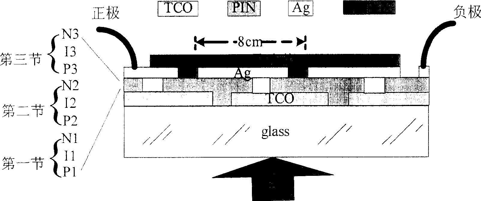
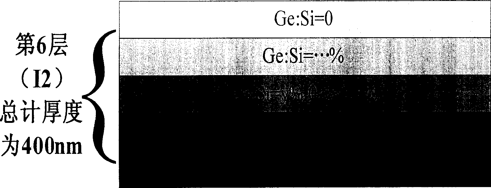
[0038] Such as figure 1 As shown, the thickness of the multilayer film of the thin film battery except the glass part is 2.1 μm. The structure is glass / TCO(200nm) / P1I1N1 / P2I2N2 / P3I3N3 / AZO(200nm) / Ag(100nm). Indium tin oxide ITO is used as a transparent film, which has conductive characteristics and can be used as an electrode of a battery. The first cell adopts p-α-SiC(100nm) / i-α-SiC(300nm) / n-α-SiC(100nm) structure, and the intermediate cell (second cell) adopts p-α-GeSi(100nm) / i-α-Ge x Si 1-x (400nm) / n-α-GeS (100nm) structure, the bottom cell (section 3) uses p-α-Si (100nm) / i-μ-Si (300nm) / n-α-Si (100nm). The thickness of AZO used in the negative electrode is 200nm, and that of Ag is 100nm. The absorption layer film is formed by PECVD reaction, and the ITO and Ag films are formed by sputtering. The glass used has a matte TCO. Deionized water is used for cleaning, megasonic cleaning is used, and laser etching and scribing are used to form a series connection of batteries...


PUM

PropertyMeasurementUnit
Band gap widthaaaaaaaaaa
Thicknessaaaaaaaaaa

Abstract

The invention relates to an adjustable band-gap thin-film solar cell based on a glass substrate and a fabricating method thereof. The invention is characterized in that materials with different band-gap structures are adopted as the absorbing layers such as Alpha-SiC, Alpha GexSi1-x, Mu-Si, and the like, so that a three-section structure is formed, thereby the light energy trapping is enhanced; different band gaps can be obtained by adopting a method for adjusting the proportion of ingredients of Ge and Si of an intrinsic layer, thereby the light energy absorption is enhanced; the energy consumption of process processing is less by adopting the PECVD (plasma enhanced chemical vapor deposition) film forming; the series connection in the cells is realized by laser scribing, the photolithographic process is not required, and the invention is suitable for batch production.

Description

technical field [0001] The invention relates to a three-section thin-film solar cell with an adjustable bandgap and a manufacturing method thereof. Specifically, three layers of materials with different bandgap widths are used as the optical absorption layer, and the absorption layer Ge of the middle second-section battery is adjusted. x Si 1-x (x=0~0.2) The ratio of Ge and Si of the material, thus splitting into multiple different similar band gaps, using transparent conductive film (TCO for short) as the positive electrode material, zinc aluminum oxide (AZO) and silver (Ag) as the negative electrode The material is glass as the light-transmitting layer. The invention belongs to the field of advanced solar cells. Background technique [0002] Silicon material is currently the dominant material for crystalline solar cells. In the cost share of finished crystalline silicon solar cells, silicon materials account for nearly 40%. The Si film thickness of amorphous silicon thin...

Claims


Application Information

Patent Timeline
IPC IPC(8): H01L31/042H01L31/075H01L31/20H01L31/046H01L31/0463H01L31/078
CPCY02E10/50Y02P70/50
Inventor 周健孙晓玮王伟谈惠祖周舟
Owner SHANGHAI INST OF MICROSYSTEM & INFORMATION TECH CHINESE ACAD OF SCI
Why Eureka
Try Eureka