
Polycrystalline-silicon carbide lamination thin-film solar cell

A technology of solar cells and polysilicon layers, applied in the field of solar cells, can solve problems such as low conversion efficiency, achieve reasonable structure, improve utilization rate, and improve photoelectric conversion efficiency

Inactive Publication Date: 2009-03-25
NANJING UNIV OF AERONAUTICS & ASTRONAUTICS
View PDF0 Cites 10 Cited by
  • Summary
  • Abstract
  • Description
  • Claims
  • Application Information

AI Technical Summary

Problems solved by technology

Since the bandgap width of silicon material is 1.12eV, the p-n junction formed by it only has a strong absorption effect on solar photons slightly higher than this energy, and the conversion efficiency of single-junction solar cells made of silicon thin films is generally lower than that of solar photons. 10%

Method used


Image

  • Polycrystalline-silicon carbide lamination thin-film solar cell
  • Polycrystalline-silicon carbide lamination thin-film solar cell
  • Polycrystalline-silicon carbide lamination thin-film solar cell

Examples


no. 1 example

[0031] The first embodiment: preparation of stacked thin film solar cells on glass substrate

[0032] Using ordinary glass as the substrate, after cleaning by standard RCA process, put it into the magnetron sputtering chamber, the background vacuum is better than 5×10 -5 Pa, the vacuum is 0.5Pa during deposition, and the ITO film with a thickness of 600nm is grown by sputtering with an ITO target with a purity of 99.99%. The substrate temperature is 300°C during sputtering, and the visible light transmittance of the grown ITO transparent conductive film is 86%. , the resistivity is about 2×10 -3 Ω·cm.

[0033] Subsequently, the sample was loaded into a hot wire chemical vapor deposition system, and a mixed gas of silane, methane, phosphine and hydrogen was introduced, wherein the ratio of silane to methane was 1:1, and the ratio of phosphine to silane was 1%. The bottom temperature is 400°C, and n-type silicon carbide with a thickness of 50nm is grown; then a mixed gas of si...

no. 2 example

[0035] Second embodiment: preparation of stacked thin film solar cells on stainless steel substrate

[0036] Using stainless steel sheet as the substrate, after cleaning by standard RCA process, put it into the magnetron sputtering chamber, the background vacuum is better than 5×10 -5 Pa, the vacuum is 0.5Pa during deposition, first grow a 400nm Ag reflective layer by sputtering with an Ag target with a purity of 99.99%, and the substrate temperature is room temperature; then grow a layer of 600nm thick Ag with a purity of 99.99% AZO film, the substrate temperature during growth is 450 °C, the visible light transmittance of the grown AZO transparent conductive film is 89%, and the resistivity is about 4×10 -3 Ω·cm.

[0037] Subsequently, the sample was loaded into a hot wire chemical vapor deposition system, and a mixed gas of silane, diborane and hydrogen was introduced, wherein the ratio of diborane to silane was 0.05%, the substrate temperature was 600°C, and the growth th...


PUM

PropertyMeasurementUnit
Resistivityaaaaaaaaaa
Thicknessaaaaaaaaaa
Carrier concentrationaaaaaaaaaa

Abstract

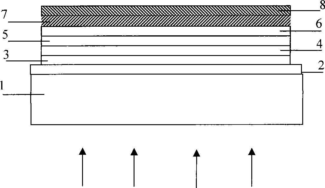
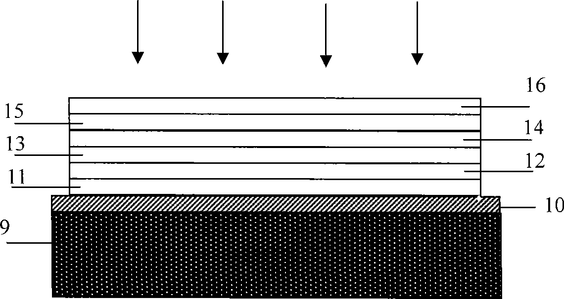
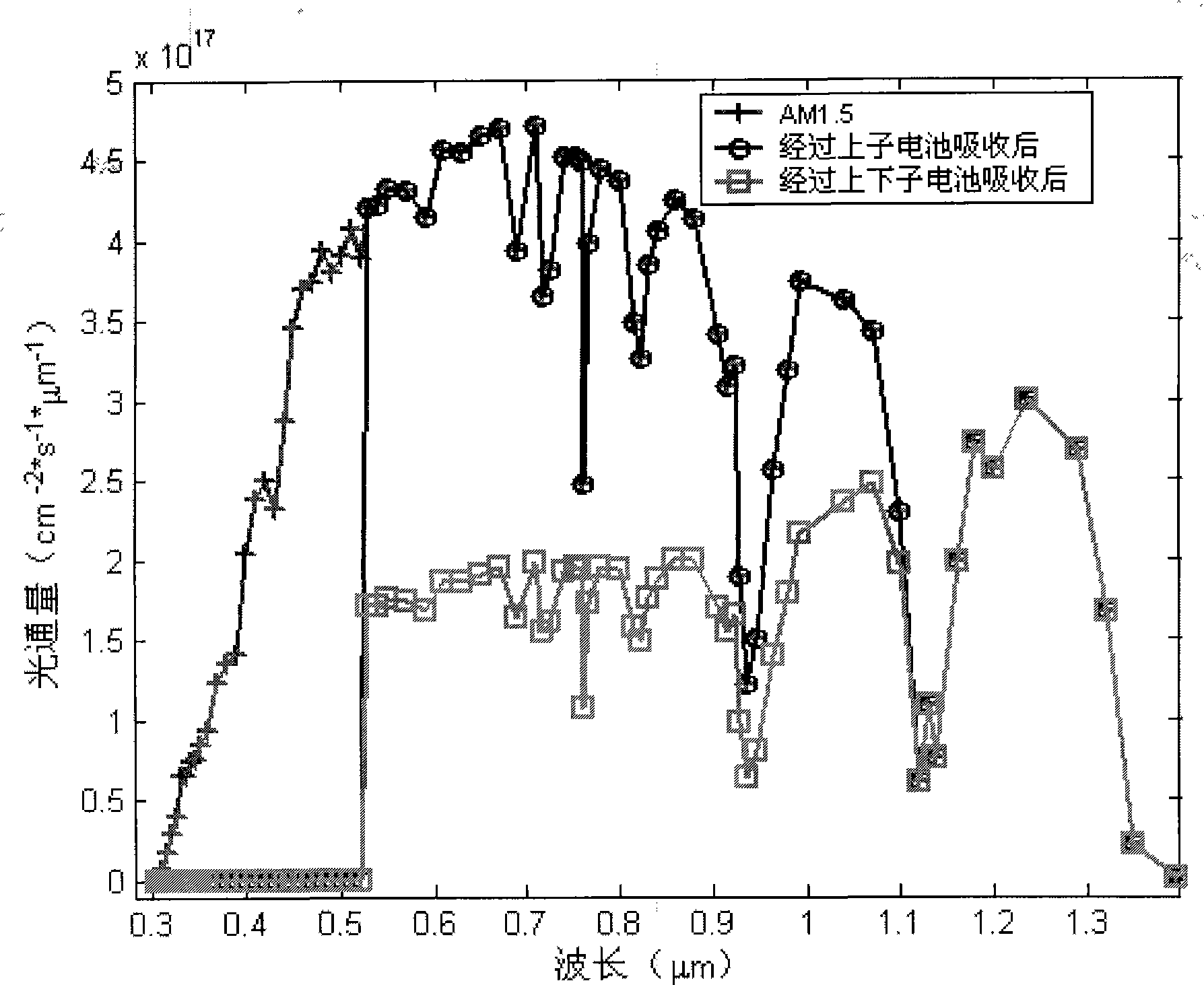
The invention discloses a polycrystalline silicon and silicon carbide stacked film solar cell, and belongs to the technical field of solar cells. The solar cell is characterized in that a glass substrate or a stainless steel substrate is taken as a substrate for the solar cell; and the solar cell comprises a transparent conductive oxide layer, the deposition of which is triggered by the magnetron sputtering, and two stack-connected film sub-solar cells prepared by using the hot filament chemical vapor deposition method on the substrate, wherein, one sub-cell is composed of a p-type silicon carbide layer / n-type silicon carbide layer, and the other sub-cell is composed of a p-type polycrystalline silicon layer / n-type polycrystalline silicon layer. The invention is characterized in that the two silicon-based materials of different band gap widths are in stack-connection with each other, so that the availability of solar spectrum and the photoelectric conversion efficiency are improved. With the inexpensive substrate and a low cost film growing source material, the invention reduces the cost of the solar cell, and gains a consequent competitive edge against a crystalline silicon solar cell.

Description

technical field [0001] The invention relates to a solar cell, in particular to a laminated thin-film solar cell which is formed by stacking two sub-cells of polycrystalline silicon and silicon carbide and can absorb broadband solar energy. Background technique [0002] Solar energy is the cleanest and most abundant energy resource bestowed by nature. At present, the conversion efficiency of commercial polysilicon solar cells is mostly around 15%. Due to the impact of rising prices of silicon raw materials, more than 55% of the cost of polysilicon solar cells is spent on silicon material substrates. From the perspective of commercial products, people have been vigorously developing low-cost, high-efficiency, large-area silicon thin-film solar cells. Since the bandgap width of silicon material is 1.12eV, the p-n junction formed by it only has a strong absorption effect on solar photons slightly higher than this energy, and the conversion efficiency of single-junction solar ce...

Claims


Application Information

Patent Timeline
IPC IPC(8): H01L31/068H01L31/0336H01L31/0687
CPCY02E10/50Y02E10/544Y02E10/546
Inventor 沈鸿烈黄海宾吴天如鲁林峰
Owner NANJING UNIV OF AERONAUTICS & ASTRONAUTICS
Learn More