

Poly-SiGe gate three-dimensional strain CMOS integrated component and preparation method thereof
An integrated device, three-dimensional technology, applied in semiconductor/solid-state device manufacturing, electric solid-state devices, semiconductor devices, etc., can solve the problem of low speed of three-dimensional integrated circuits, achieve the effect of ensuring AC and DC electrical performance, improving performance, and avoiding influence
- Summary
- Abstract
- Description
- Claims
- Application Information
AI Technical Summary
Problems solved by technology
Method used
Image

Examples
Embodiment 1
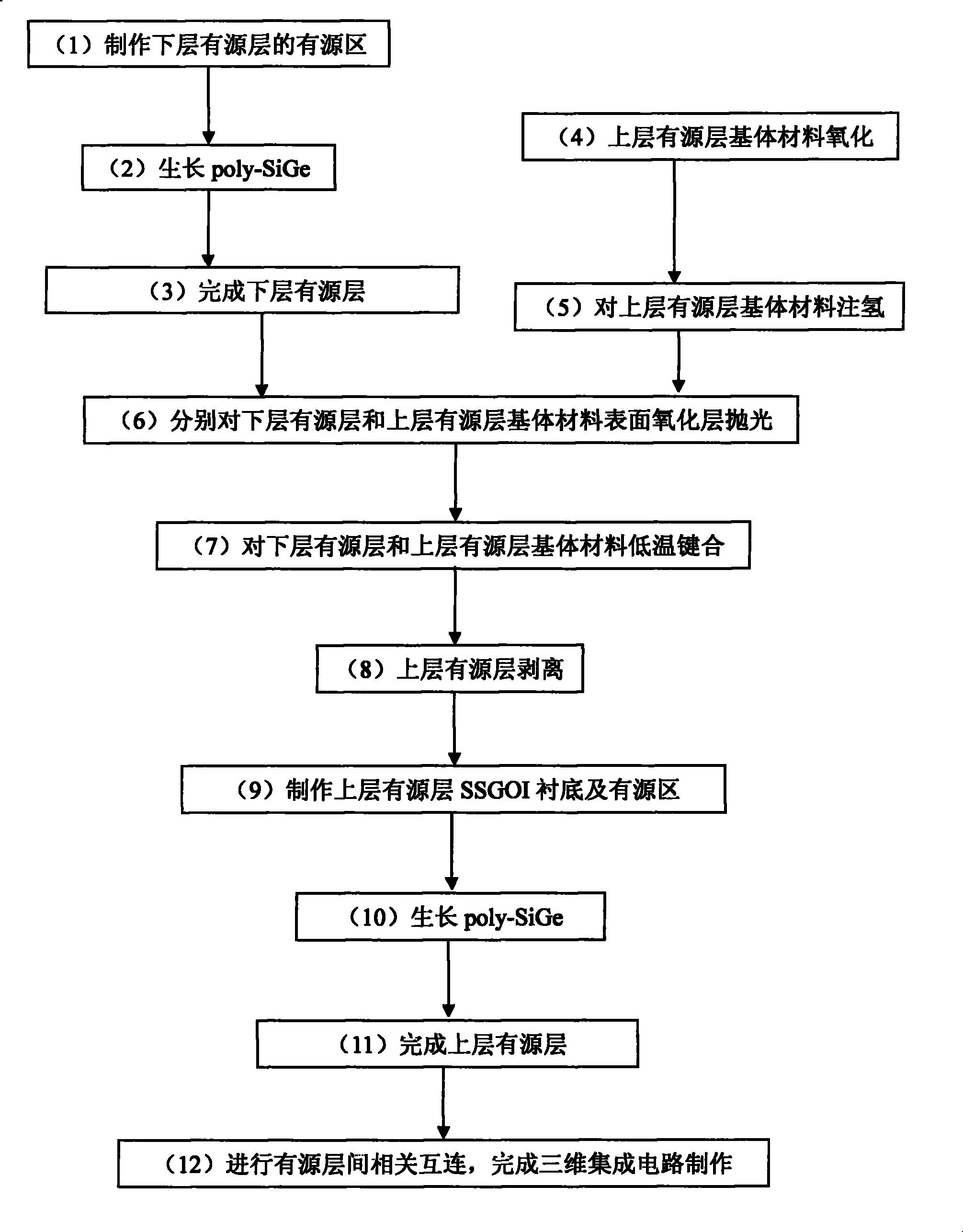
[0043] Embodiment 1: The steps of making a Poly-SiGe gate three-dimensional strained CMOS integrated device with a conductive channel of 65nm are as follows:
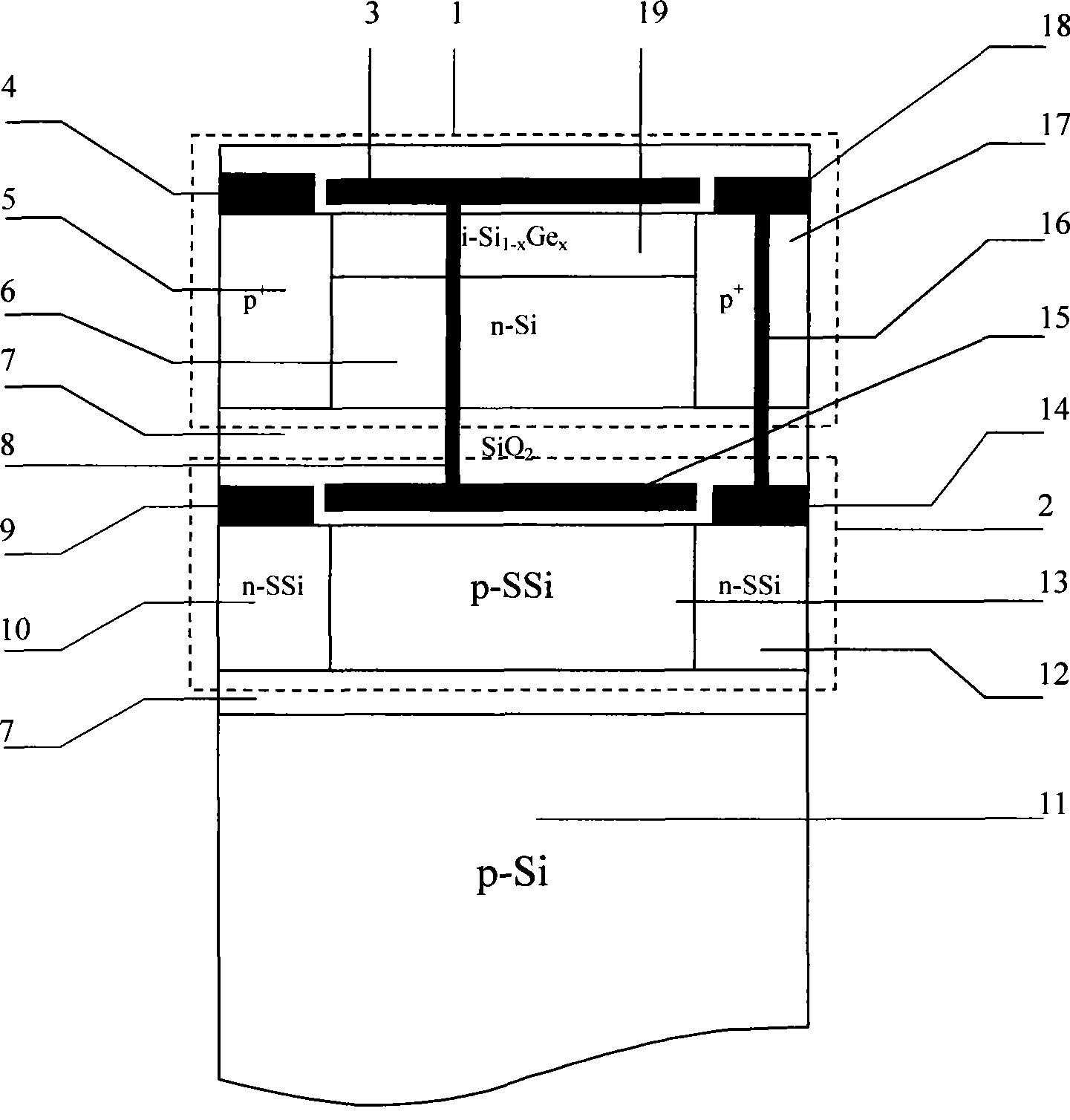
[0044] (1) Select SSOI substrates with stress>1Gpa;
[0045] (2) On the SSOI substrate, the active area is produced by oxidation, photolithography, ion implantation and other processes;
[0046] (3) Using ultra-high vacuum chemical vapor deposition UHVCVD method, a layer of p-type Poly-SiGe is deposited on the active region as the gate, and the doping concentration is >10 20 cm -3 , Ge composition is 0.2;
[0047] (4) On the Poly-SiGe layer, through photolithography Poly-SiGe layer-passivation-ion implantation-lithography lead hole-polysilicon wiring-low temperature deposition of SiO 2 The dielectric layer is used to make a strained Si nMOSFET device structure and interconnection with a Poly-SiGe gate with a conductive channel of 65nm;
[0048] (5) Deposit SiO on the surface of the lower active layer 2 medium layer...
Embodiment 2
[0059] Embodiment 2: The steps of making a Poly-SiGe gate three-dimensional strained CMOS integrated device with a conductive channel of 90nm are as follows:
[0060] (1) Select SSOI substrates with stress>1Gpa;
[0061] (2) On the SSOI substrate, the active area is produced by oxidation, photolithography, ion implantation and other processes;
[0062] (3) Using the reduced pressure chemical vapor deposition RPCVD method, a layer of p-type Poly-SiGe is deposited on the active region as the gate, and the doping concentration is >10 20 cm -3 , Ge composition is 0.05;
[0063] (4) On the Poly-SiGe layer, through photolithography Poly-SiGe layer-passivation-ion implantation-lithography lead hole-polysilicon wiring-low temperature deposition of SiO 2 The dielectric layer is used to make a strained Si nMOSFET device structure and interconnection with a poly-SiGe gate with a conductive channel of 90nm;
[0064] (5) Deposit SiO on the surface of the lower active layer 2 medium la...
Embodiment 3
[0075] Embodiment 3: The steps of making a Poly-SiGe gate three-dimensional strained CMOS integrated device with a conductive channel of 130nm are as follows:
[0076] (1) Select SSOI substrates with stress>1Gpa;
[0077] (2) On the SSOI substrate, the active area is produced by oxidation, photolithography, ion implantation and other processes;
[0078] (3) Using ultraviolet photochemical vapor deposition UVCVD method, deposit a layer of p-type Poly-SiGe on the active region, as the gate, doping concentration > 10 20 cm -3 , Ge composition is 0.3;
[0079] (4) On the Poly-SiGe layer, through photolithography Poly-SiGe layer-passivation-ion implantation-lithography lead hole-polysilicon wiring-low temperature deposition of SiO 2 The dielectric layer is used to make a strained Si nMOSFET device structure and interconnections with a Poly-SiGe gate with a conductive channel of 130nm;
[0080] (5) Deposit SiO on the surface of the lower active layer 2 medium layer;
[0081] (...
PUM
 Abstract
Description
Claims
Application Information