Shallow slot preparing method

A technology of shallow trenches and trenches, applied in semiconductor/solid-state device manufacturing, electrical components, circuits, etc., can solve problems that are not conducive to device gate oxide layer thinning effect device leakage current, and achieve the effect of reducing leakage current

Inactive Publication Date: 2009-05-06
SHANGHAI HUA HONG NEC ELECTRONICS
View PDF0 Cites 10 Cited by
  • Summary
  • Abstract
  • Description
  • Claims
  • Application Information

AI Technical Summary

Problems solved by technology

However, this process has a disadvantage, that is, it usually makes the shape of the top corner of the STI very sharp, forming such as image 3 and Figure 7 The top s

Method used


Image

  • Shallow slot preparing method
  • Shallow slot preparing method
  • Shallow slot preparing method

Examples


Embodiment Construction

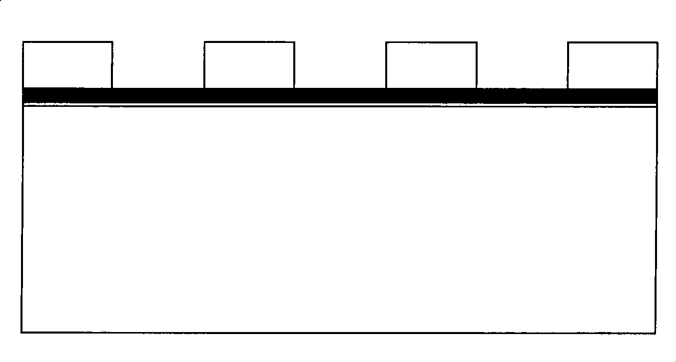
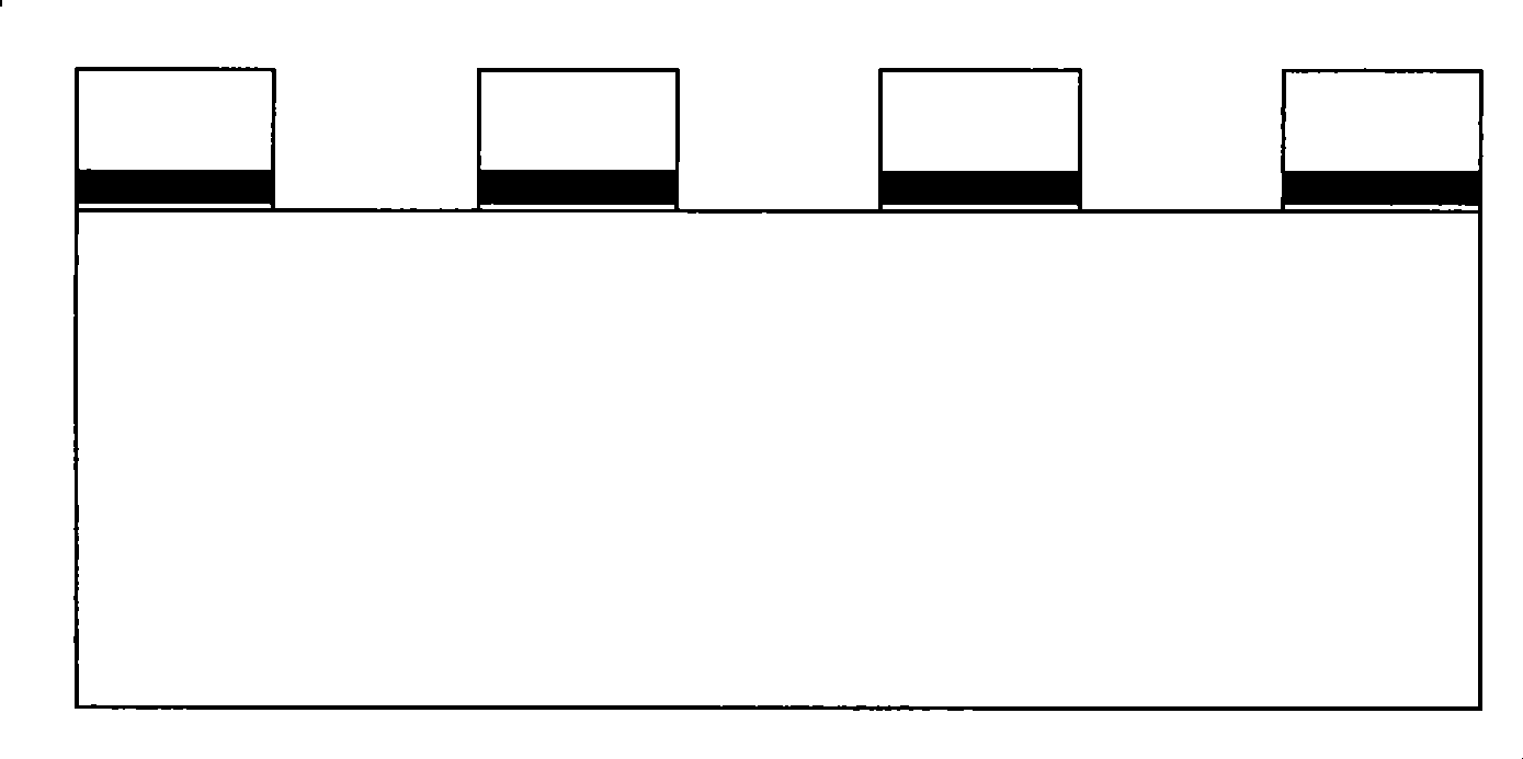
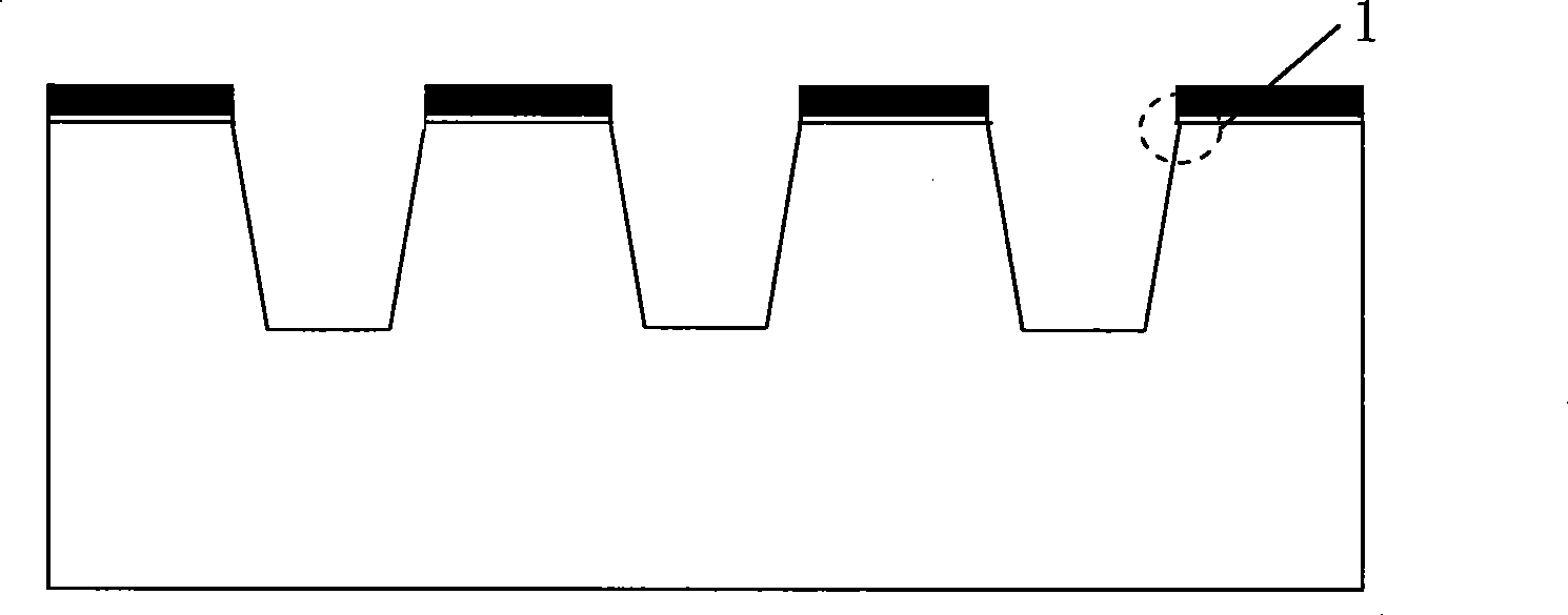
[0042] Such as Figure 16 Shown is the process flow diagram of the present invention, the shallow trench preparation method of the present invention first grows a pad oxide layer (silicon dioxide) on a substrate (silicon wafer), and deposits a hard mask layer (silicon nitride) . Next is the photoresist coating and exposure development of the active area, which will require the area (field area) outside the device to be opened (such as Figure 8 shown). Then the hard mask layer is etched, and the silicon nitride mask (hard mask) in the field area is removed and the photoresist is stripped by etching with silicon nitride plasma. Subsequent anisotropic wet etching of silicon wafers, such as Figure 9 As shown, since the anisotropic etching solution will not react with silicon nitride, the silicon surface will be etched only in the area without silicon nitride. Since the etching rate of the anisotropic etching solution is different in each crystal direction, so A slope of abou...


PUM

PropertyMeasurementUnit
Thicknessaaaaaaaaaa

Abstract

The invention discloses a preparation method of a shallow groove, which comprises the following steps: growing a cushion oxide layer on an underlay; successively depositing a hard mask layer; etching coating cloth, exposing and developing; etching the hard mask layer and removing a photoresist; carrying out anisotropic wet etching; carrying out dry etching and forming the groove on the underlay; eroding the cushion oxide layer of a corner at the top end of the groove; growing the cushion oxide layer in the groove of the underlay in a thermal oxidation manner; filling an HDP oxide layer; and carrying out chemical-mechanical grinding and removing the hard mask layer. Because the anisotropic wet etching process is added before the dry etching step, the tilting angle of the corner at the top end of STI is lessened; furthermore, the top part of the STI is polished during the process of the cushion oxide layer of the corner at the top end of the corrosive groove; and finally the novel smooth appearance of the corner at the top end of the STI is obtained, thereby the thinning effect and the narrow-channel effect of the grid oxide layer of the device are improved or overcome, and the leakage current of the device is reduced.

Description

technical field [0001] The invention relates to a manufacturing process of a semiconductor device, in particular to a method for preparing a shallow trench. Background technique [0002] Shallow trench isolation technology (Shallow Trench Isolation) is a device isolation technology widely used in VLSI, such as Figure 1 to Figure 7 As shown, the process is mainly as follows: [0003] (1) growing a pad oxide layer on the substrate, and then depositing a hard mask layer; [0004] (2) Photoresist coating and exposure development (such as figure 1 ); [0005] (3) hard mask layer etching and removal of photoresist (such as figure 2 ); [0006] (4) Dry etching to form grooves on the substrate (such as image 3 ); [0007] (5) corrode the liner oxide layer at the top corner of the trench; [0008] (6) Thermal oxygen growth pad oxide layer in the groove of the substrate (such as Figure 4 ); [0009] (7) Carry out HDP oxide layer filling (such as Figure 5 ); [0010] (...

Claims


Application Information

Patent Timeline
IPC IPC(8): H01L21/762
Inventor 陈华伦陈瑜熊涛罗啸陈雄斌
Owner SHANGHAI HUA HONG NEC ELECTRONICS
Why Eureka
Try Eureka