

Implementation of avalanche photo diodes in (BI) CMOS processes
A photodiode and process technology, applied in the field of medical imaging, can solve problems such as large volume, design rule obstruction, poor working effect, etc., and achieve the effect of increasing detection efficiency
- Summary
- Abstract
- Description
- Claims
- Application Information
AI Technical Summary
Problems solved by technology
Method used
Image

Examples
Embodiment Construction
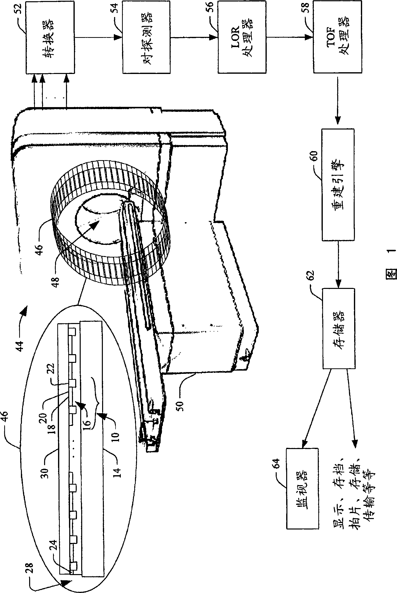
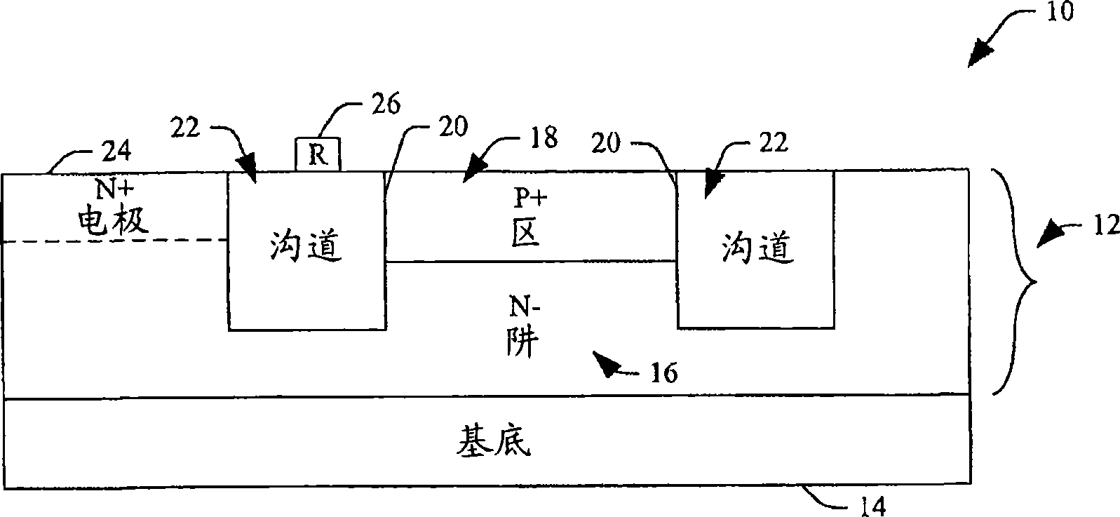
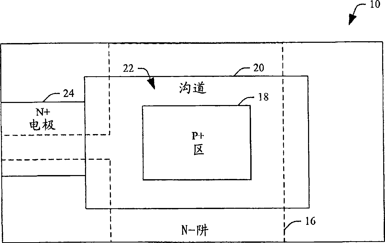
[0023] refer to figure 2 with 3 , which show photodiodes 10 fabricated to suppress, reduce, eliminate, etc., the premature edge breakdown associated with conventional photodiodes driven in conventional Geiger or other modes, such as avalanche photodiodes (APDs). . figure 2 depicts a side view of photodiode 10, image 3 A top view of photodiode 10 is depicted.
[0024] Photodiode 10 includes a semiconductor layer 12 (e.g., silicon (Si), germanium (Ge), gallium arsenide (GaAs), etc.) formed (e.g., by photolithography, lithography, etc.) on on a substrate 14 (eg, silicon, glass, sapphire, etc. wafer). The semiconductor layer 12 includes an n-type (n-doped) well 16 arranged adjacent to a p-type (p+ doped) region 18 between which a pn junction is formed. Such regions are formed by known techniques such as ion implantation (where ions are implanted, thereby altering the physical properties of semiconductor layer 12), diffusion, and / or the like.
[0025] A channel 20 is forme...
PUM
 Abstract
Description
Claims
Application Information