
Eureka
For R&D, Eureka makes reading and utilizing patents & technical documents easy.
Eureka AIR
Designed for self-driven R&D workflows. Generate viable solutions, solve complex R&D challenges, empower your innovation with AI.

Eureka Materials
Designed for material experts only. Revolutionize your material R&D, from search, analyze, to developing new materials.

TechResearch
Generate reliable direction feasibility study reports for your R&D in just a few steps.

TechSeek
Discover and master advanced knowledge NOW. Basics, ideas, possibilities, all at once.

TechMind
As an expert in R&D Theories, TechMind can generates customized viable solutions instantly.

TechRisk
Analyze your overall solution with one click, know your potential R&D risks in advance.

TechMonitor
Get weekly tech updates, stay abreast of the latest tech innovations and key insights.
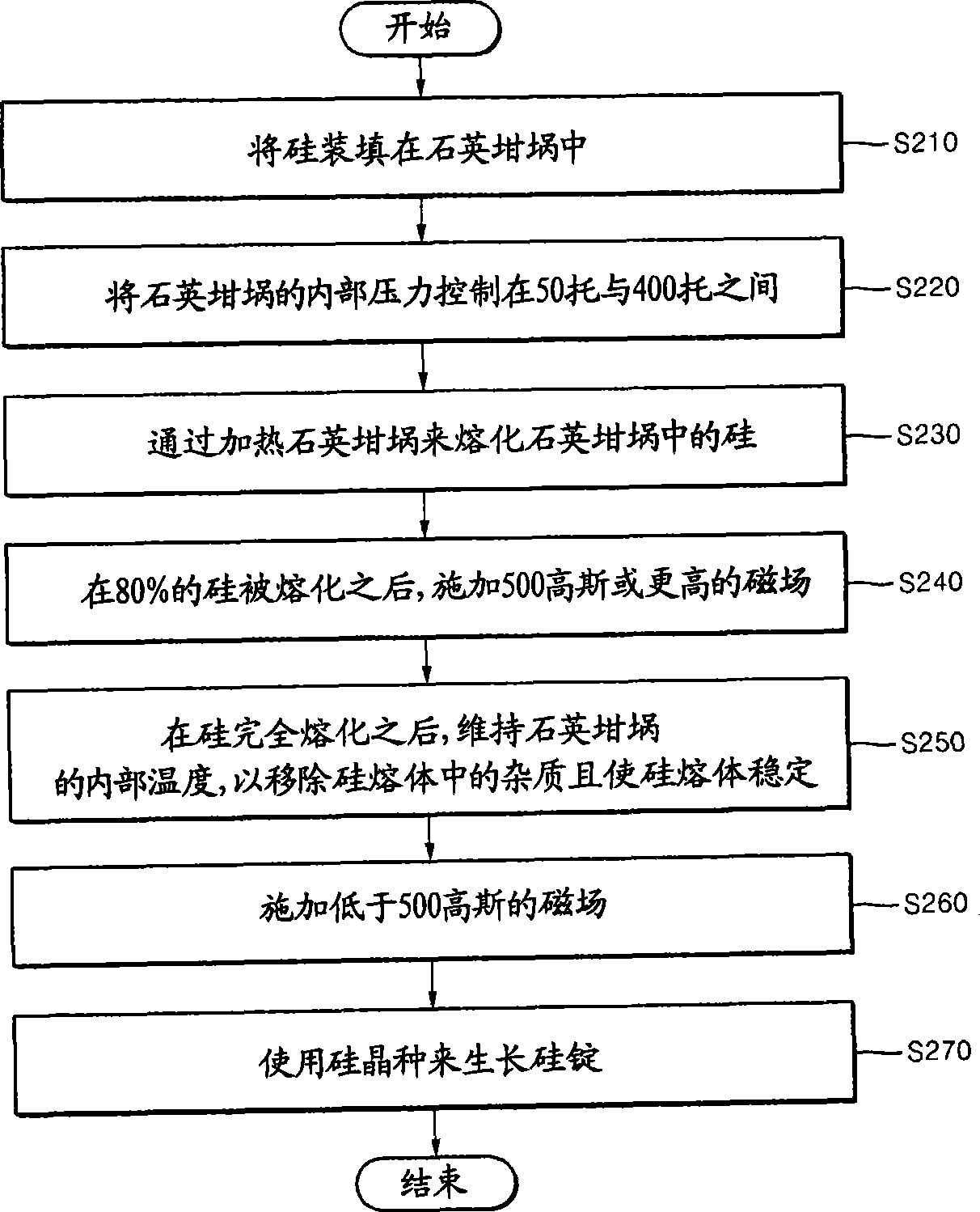
Method for growing silicon ingot
A technology for silicon ingots and single-crystal silicon ingots, applied in the directions of crystal growth, single crystal growth, single crystal growth, etc., can solve problems such as increasing process costs, and achieve the effects of improving characteristics and yield, preventing peeling, and good characteristics
- Summary
- Abstract
- Description
- Claims
- Application Information
AI Technical Summary
Problems solved by technology
Method used
Image

Examples
Embodiment Construction
[0021] Hereinafter, specific embodiments will be described in detail with reference to the accompanying drawings. This invention may, however, be embodied in different forms and should not be construed as limited to the embodiments set forth herein. Rather, these embodiments are provided so that this disclosure will be thorough and complete, and will fully convey the scope of the invention to those skilled in the art. In the drawings, the shapes of elements are exaggerated for clarity of illustration, and like reference numerals refer to like elements throughout.
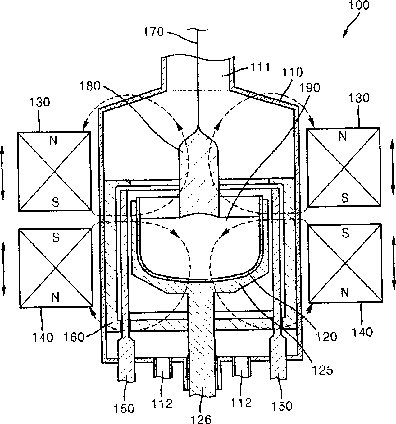
[0022] figure 1 is a schematic cross-sectional view of a silicon ingot growing apparatus used in a method for growing a silicon ingot according to an exemplary embodiment.
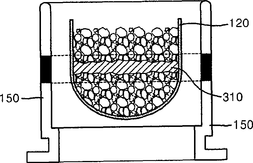
[0023] see figure 1 As shown, silicon ingot growing apparatus 100 includes main body 110 , quartz crucible 120 , support 125 , upper electromagnet 130 , lower electromagnet 140 , heater 150 , insulating wall 160 and cables 170 .
[0024] The...
PUM
 Abstract
Description
Claims
Application Information
 - R&D Engineer
- R&D Manager
- IP Professional
- Industry Leading Data Capabilities
- Powerful AI technology
- Patent DNA Extraction
Browse by: Latest US Patents, China's latest patents, Technical Efficacy Thesaurus, Application Domain, Technology Topic, Popular Technical Reports.
© 2024 PatSnap. All rights reserved.Legal|Privacy policy|Modern Slavery Act Transparency Statement|Sitemap|About US| Contact US: help@patsnap.com