Group III nitride compound semiconductor LED and production method thereof

A technology of light-emitting diodes and manufacturing methods, which is applied to semiconductor devices, electrical components, circuits, etc., and can solve problems affecting the quality of crystal epitaxial growth, etc.

Inactive Publication Date: 2009-06-10
ZHANJING TECH SHENZHEN +1
View PDF3 Cites 16 Cited by
  • Summary
  • Abstract
  • Description
  • Claims
  • Application Information

AI Technical Summary

Problems solved by technology

However, the AlN non-planar layer 34 needs a special heat treatment process to be formed on the N-type c

Method used


Image

  • Group III nitride compound semiconductor LED and production method thereof
  • Group III nitride compound semiconductor LED and production method thereof
  • Group III nitride compound semiconductor LED and production method thereof

Examples


Embodiment Construction

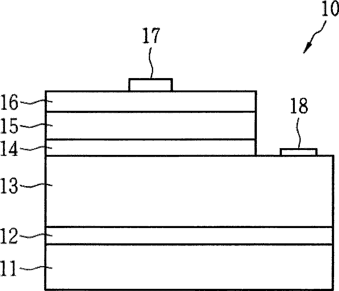
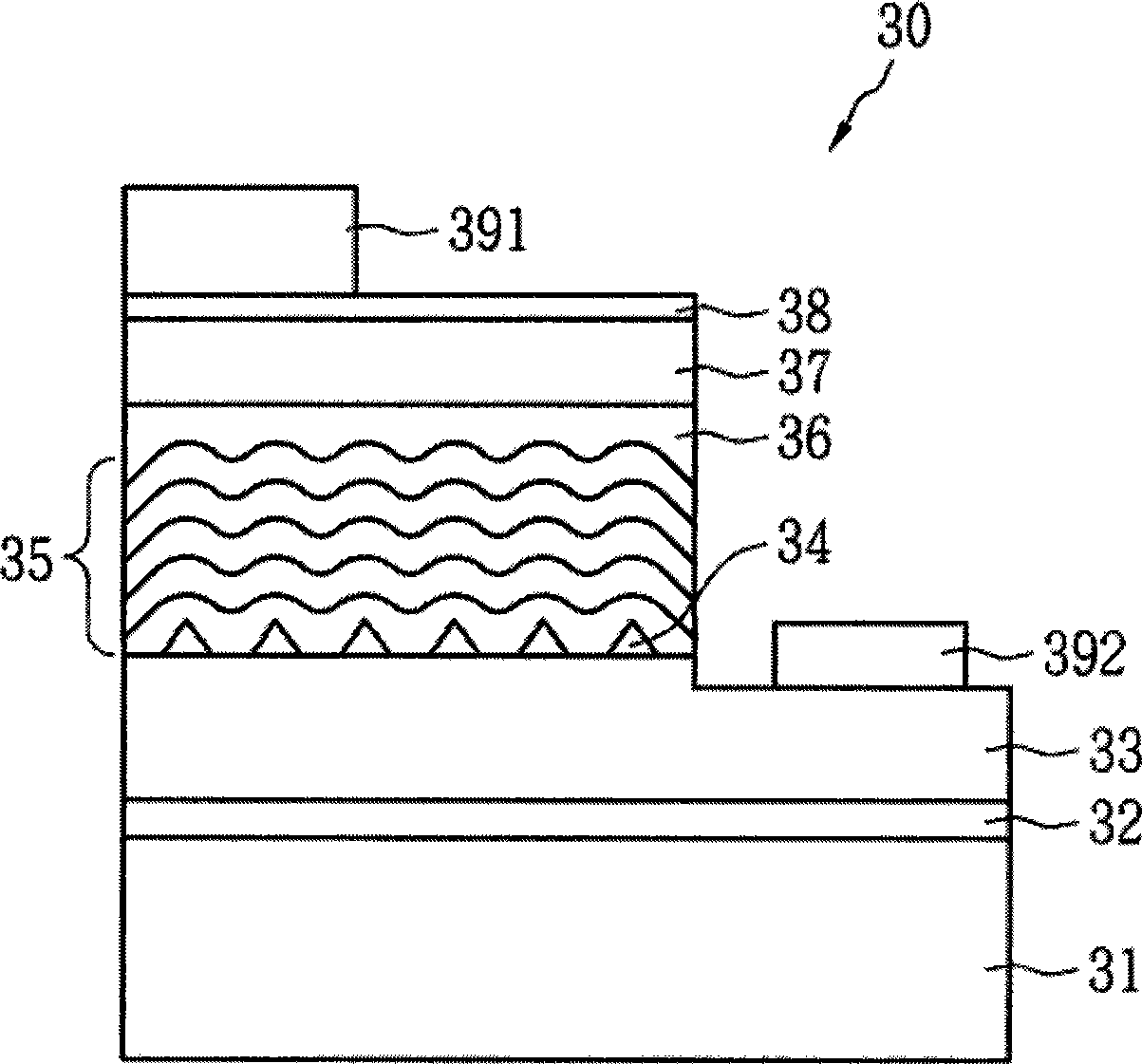
[0025] Figure 4 It is a schematic cross-sectional view of a Group III nitrogen compound semiconductor light-emitting diode of the present invention. The light-emitting diode 40 includes a substrate 41, a buffer layer 42, an N-type (or called first-type) semiconductor material layer 43, a conformal active layer 44, and a P-type (or called second-type) semiconductor material layer 45. An N-type electrode 47 is provided on the surface of the N-type semiconductor material layer 43 , and a P-type electrode 46 is provided on the surface of the P-type semiconductor material layer 45 .

[0026] Generally speaking, to manufacture the light emitting diode 40, a substrate 41 is firstly provided, such as: sapphire (that is, aluminum oxide compound Al 2 o 3 ), silicon carbide (SiC), silicon, zinc oxide (ZnO), magnesium oxide (MgO), gallium arsenide (GaAs), etc., and different material layers are formed on the substrate 41 . Because the substrate 41 does not match the lattice constant o...


PUM

PropertyMeasurementUnit
Widthaaaaaaaaaa

Abstract

The invention provides a three-group nitrogen-compound semiconductor LED, which comprises a substrate, a buffer layer, an N-type semiconductor material layer, conformation active layers and a P-type semiconductor material layer, wherein the N-type semiconductor material layer has a first surface and a second surface; the first surface is in direct contact with the buffer layer; the second surface has a plurality of concave parts; the conformation active layers are formed on the second surface and in the concave parts; and the stress between the conformation active layers and the N-type semiconductor material layer can be released through the concave parts.

Description

technical field [0001] The invention relates to a group III nitrogen compound semiconductor light emitting diode and its manufacturing method, in particular to a group III nitrogen compound semiconductor light emitting diode capable of releasing stress between an active layer and an N-type semiconductor material layer and its manufacturing method. Background technique [0002] As light-emitting diode elements are widely used in different products, in recent years, materials for making blue light-emitting diodes have become an important research and development object in the current optoelectronic semiconductor material industry. At present, the materials of blue light-emitting diodes include zinc selenide (ZnSe), silicon carbide (SiC) and indium gallium nitride (InGaN). above eV. Since the gallium nitride series is a light-emitting material with a direct gap, it can produce high-brightness illumination light, and has the advantage of longer life than zinc selenide, which al...

Claims


Application Information

Patent Timeline
IPC IPC(8): H01L33/00H01L33/02H01L33/12
Inventor 涂博闵黄世晟叶颖超林文禹吴芃逸徐智鹏詹世雄
Owner ZHANJING TECH SHENZHEN
Why Eureka
Try Eureka