Preparation of semiconductor and metal quasi-one-dimensional nano heterogeneous cycle structure array

A periodic structure and semiconductor technology, applied in the direction of nanostructure manufacturing, nanotechnology, nanotechnology, etc., can solve the problems of high cost, process replication, etc., and achieve the effect of large aspect ratio and low cost of preparation materials

Inactive Publication Date: 2009-07-22
JILIN UNIV
View PDF0 Cites 20 Cited by
  • Summary
  • Abstract
  • Description
  • Claims
  • Application Information

AI Technical Summary

Problems solved by technology

Among these preparation methods, the electrodeposition method is more extensive than other methods, but the currently used electrodeposition method is to place the alumina template in the solution first, and control the different deposition potentials to make the ions in the pores of the alumina template Electrodeposition is carried out in the medium, and then the alumina template is removed by chemical treatment to obtain a quasi-one-dimensional semiconductor nanostructure material. In this preparation process, the process is relatively duplicated and the cost is high; t

Method used


Image

  • Preparation of semiconductor and metal quasi-one-dimensional nano heterogeneous cycle structure array
  • Preparation of semiconductor and metal quasi-one-dimensional nano heterogeneous cycle structure array
  • Preparation of semiconductor and metal quasi-one-dimensional nano heterogeneous cycle structure array

Examples


Embodiment 1

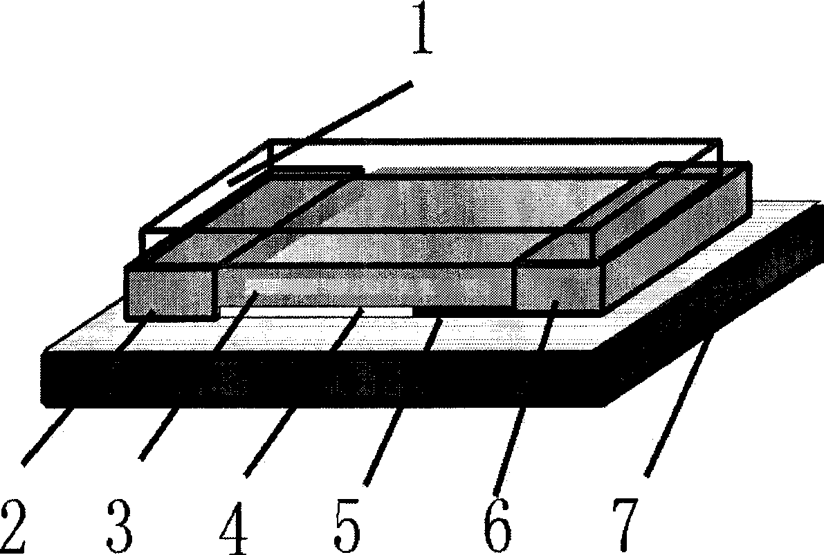
[0043] Example 1 Combined figure 1 Describe a kind of device structure that the present invention adopts

[0044] When the present invention prepares semiconductor and metal quasi-one-dimensional nano-heterogeneous periodic structure array materials, a device suitable for the preparation method of the present invention-a semi-closed electrolytic cell is used, and the schematic diagram of the device after placing the solution, electrodes and substrates Such as figure 1 shown. figure 1 Among them, 1 is the cover glass, 2 is the anode, 3 is the ice layer, 4 is the thin liquid layer, 5 is the sediment, 6 is the cathode, and 7 is the surface-treated single crystal silicon wafer. The ice layer 3 is formed after cooling in the temperature control system, and the temperature control system may be a low-temperature circulation chamber device. The two lead foil electrodes 2 and 6 can be respectively connected to the positive and negative ends of the waveform generator when preparing ...

Embodiment 2

[0045] Example 2 Preparation method of PbSe and Pb quasi-one-dimensional nanoheterogeneous periodic structure array material

[0046] with deionized water and lead nitrate and SeO 2 The configuration contains 0.03M / L Pb 2+ and 0.005M / L HSeO 2 + electrolyte, and then adjust the pH of the solution to 0.95 with nitric acid. Use metallic lead foil as the electrode, with a thickness of 100 μm and a length of 2 cm. Using a silicon single wafer cleaned by a standard semiconductor cleaning process as a substrate to assemble an electrolytic cell, the device is as follows figure 1 Then put it into the temperature control system, control the temperature at -5.25°C through a water bath, and freeze the electrolyte in the electrolytic cell. When the thickness of the liquid layer reaches 100nm, the square wave voltage edited by the waveform generator is applied to the electrodes to prepare PbSe and Pb quasi-one-dimensional nanostructure materials. The high potential of the applied squar...

Embodiment 3

[0047] Example 3 Preparation method of PbTe and Pb quasi-one-dimensional nanoheterogeneous periodic structure array material

[0048] with deionized water and lead nitrate and TeO 2 The configuration contains 0.02M / L Pb 2+ and 0.001M / L HTeO 2 + Electrolyte, and then use nitric acid to adjust the pH value of the solution to 1.2. Use metallic lead foil as the electrode, with a thickness of 100 μm and a length of 2 cm. Using a silicon single wafer cleaned by a standard semiconductor cleaning process as a substrate to assemble an electrolytic cell, the device is as follows figure 1 Then put it into the temperature control system, control the temperature at -4.50°C through a water bath, and refrigerate the electrolytic cell to freeze the electrolyte. When the thickness of the electrolyte layer reaches 100nm, the square wave edited by the waveform generator is applied to the electrode to prepare PbTe and Pb quasi-one-dimensional nanostructure materials. The high potential of th...


PUM

PropertyMeasurementUnit
Heightaaaaaaaaaa
Thicknessaaaaaaaaaa
Lengthaaaaaaaaaa

Abstract

The invention pertains to the technical field of preparing semiconductor and metal quasi-one-dimensional nanometer heterogeneous cycle structure array material by an electrochemical deposition method. The semiconductor is PbTe or PbSe and the metal is Pb. The preparation process is as follows: an electrolyte containing Pb and HTeO or HSeO is prepared and poured between two lead foil electrodes in a semi-enclosed electrolytic cell; the electrolyte is cooled and frozen at the temperature between minus 3.0 DEG C and minus 7.0 DEG C; square wave is exerted on the electrodes; deionized water is applied to cleaning the base after preparation; and the semiconductor and the metal quasi-one-dimensional nanometer heterogeneous cycle structure array material are obtained. The invention has low preparation cost and needs no template; the material has large length-diameter ratio, and lines are in parallel arrangement; the structure of the material can be controlled by freezing temperature and square wave voltage.

Description

technical field [0001] The invention belongs to the technical field of preparing quasi-one-dimensional semiconductor and metal nano-heterogeneous periodic structure array materials by electrochemical deposition, and especially relates to the manufacture of large-area semiconductor and metal nano-structures with a large aspect ratio on a two-dimensional plane. Methods for Heterogeneous Periodic Structured Array Materials. Background technique [0002] Semiconductor nanostructured materials are widely used in basic research and the construction of nanodevices. With the reduction of material scale, unique properties are exhibited. In particular, one-dimensional semiconductor nanostructured materials have great potential in one-dimensional waveguide, thermoelectricity, laser and detection. Various applications. Among semiconductor materials, PbSe and PbTe are important narrow energy band and strong confinement semiconductor materials, and their luminescence covers the near and ...

Claims


Application Information

Patent Timeline
IPC IPC(8): B82B3/00
Inventor 张明喆宗兆存王双明邹广田
Owner JILIN UNIV
Why Eureka
Try Eureka