

Honeycomb CuO nano material and preparation thereof
A honeycomb and nanotechnology, applied in the field of nanomaterials, can solve few problems and achieve the effect of novel method, low cost and simple method
- Summary
- Abstract
- Description
- Claims
- Application Information
AI Technical Summary
Problems solved by technology
Method used
Image

Examples
Embodiment 1
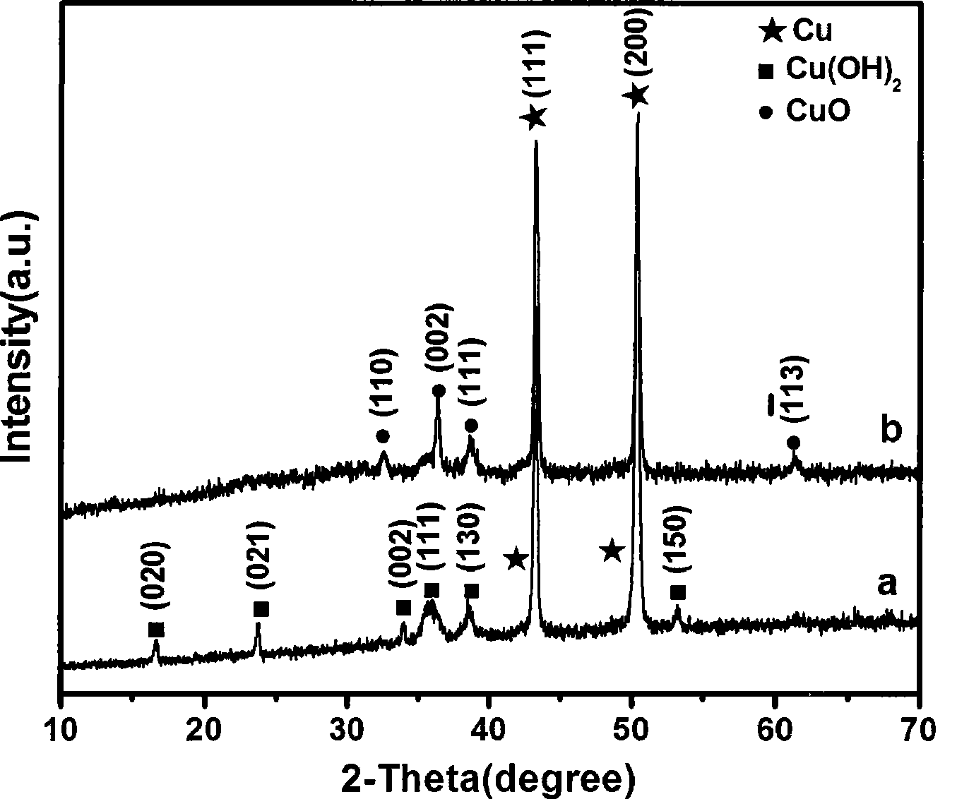
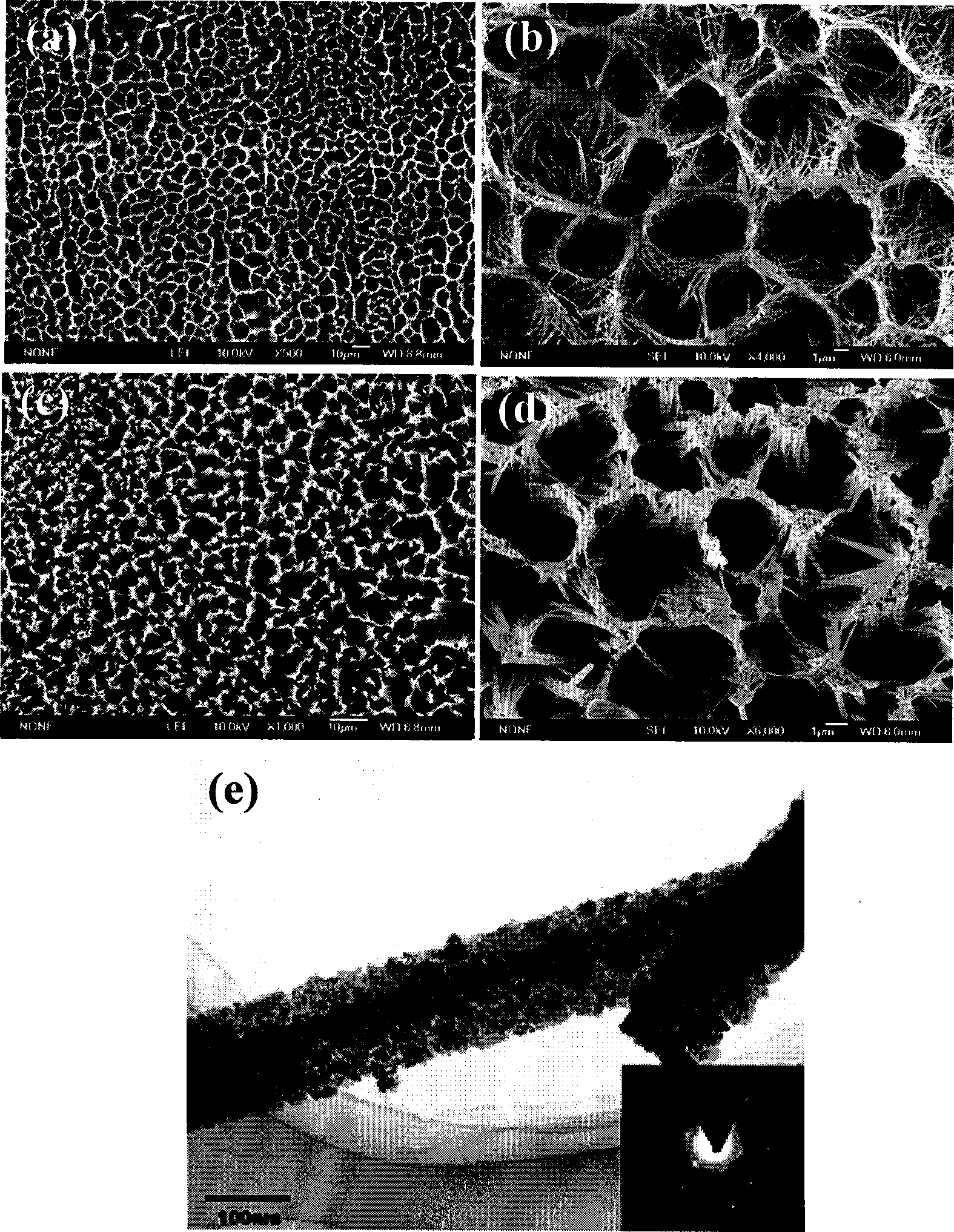
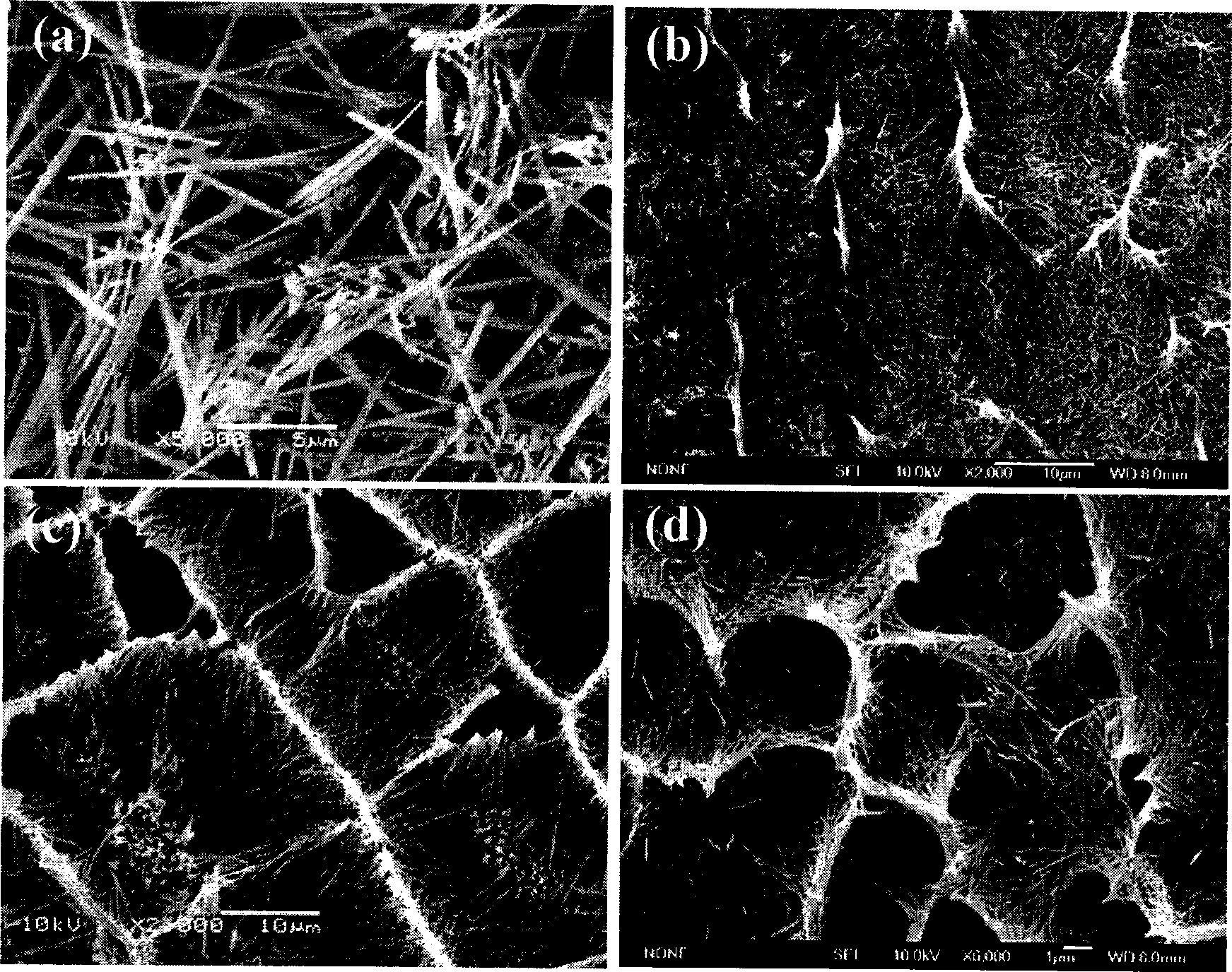
[0019] Set the surface area to 1.5cm 2 The copper sheet is polished, soaked in 30% hydrochloric acid for 8 minutes, and then put into acetone for ultrasonication, and the obtained pure copper sheet is used as the anode; the selected surface area is about 1.6cm 2 Graphite (as cathode; 3mol / L KOH as electrolyte; voltage 3V; 3h after electrodeposition; take out the copper sheet, you can see a layer of blue Cu(OH) on the surface of the copper sheet 2 Precursor; in N 2 Under protection, the obtained Cu(OH) 2 The precursor was heated at 150°C for 2.5h, and then taken out, a layer of black honeycomb nano-CuO was formed on the surface of the copper sheet.
Embodiment 2
[0021] Place a copper sheet (approximately 1.5 cm in surface area) 2 ) polished, soaked in 30% hydrochloric acid for 10 minutes, and then placed in acetone for ultrasonication, the obtained pure copper sheet was used as an anode; graphite (surface area about 1.6cm 2 ) as the cathode; 3mol / L KOH as the electrolyte; the voltage is 5V; after 5 hours of electrodeposition; take out the copper sheet, and you can see that a layer of blue Cu(OH) is formed on the surface of the copper sheet 2 Precursor; in N 2 Under protection, the obtained Cu(OH) 2 The precursor was heated at 160°C for 3.5h, and then taken out, a layer of black honeycomb nano-CuO was formed on the surface of the copper sheet.
Embodiment 3
[0023] Place a copper sheet (approximately 1.5 cm in surface area) 2 ) polished, soaked in 30% hydrochloric acid for 9 minutes, and then placed in acetone for ultrasonication, and the obtained pure copper sheet was used as an anode; graphite (surface area about 1.6cm 2 ) as the cathode; 3mol / L KOH as the electrolyte; the voltage is 4V; after 4 hours of electrodeposition; take out the copper sheet, and you can see that a layer of blue Cu(OH) is formed on the surface of the copper sheet 2 Precursor; in N 2 Under protection, the obtained Cu(OH) 2 The precursor was heated at 155°C for 3 hours, and then taken out, a layer of black honeycomb nano-CuO was formed on the surface of the copper sheet.
PUM
| Property | Measurement | Unit |
|---|---|---|
| length | aaaaa | aaaaa |
| diameter | aaaaa | aaaaa |
| thickness | aaaaa | aaaaa |
Abstract
Description
Claims
Application Information