Nano-scale printing mould structure and its use on luminous element

A nano-scale, stamping technology, applied in electrical components, optics, opto-mechanical equipment, etc., can solve the problems of limited extraction efficiency of light-emitting diodes, time-consuming production, and high prices.

Active Publication Date: 2009-07-22
EPISTAR CORP
View PDF3 Cites 6 Cited by
  • Summary
  • Abstract
  • Description
  • Claims
  • Application Information

AI Technical Summary

Problems solved by technology

The common method of making impressions is to use electron beam lithography direct writing or ion photolithography to make them, but because of the time-consuming production, the price remains high
In addition, most of this type of die is a step-profile up-and-down pattern. Although it can be applied to the control of the output light of LEDs (such as photonic crystals), it is of limited help to the extraction efficiency of LEDs. Because the light of the light-emitting diode is mostly emitted from the sidewall of the nanostructure

Method used


Image

  • Nano-scale printing mould structure and its use on luminous element
  • Nano-scale printing mould structure and its use on luminous element
  • Nano-scale printing mould structure and its use on luminous element

Examples


Embodiment 1

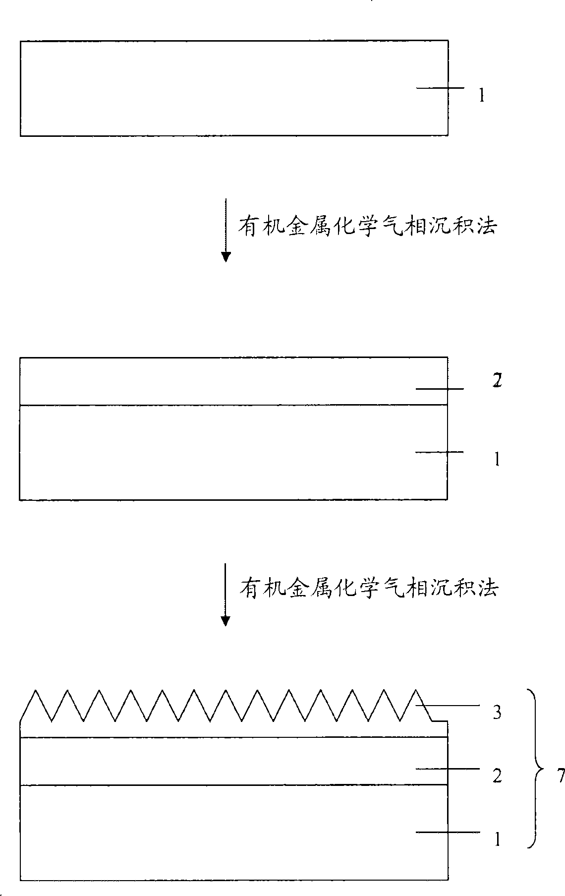
[0033] Such as figure 2 As shown, a buffer layer 2 formed, for example, by undoped gallium nitride (u-GaN) is grown on an aluminum oxide (Sapphire) substrate 1 by metal organic chemical vapor deposition (MOCVD); a stamp layer 3, Among them, for example, it is undoped gallium nitride (u-GaN) or n-type doped gallium nitride (n-GaN), and the thickness of the stamp layer is at least 5000 Angstroms ( ). By adjusting the production parameters of the organic metal chemical vapor deposition method, the upper surface of the stamp layer can form a zigzag (triangular) pattern with a size of 10nm to 1000nm and a period of 20nm to 2000nm. Nanoscale stamp structure7 .

Embodiment 2

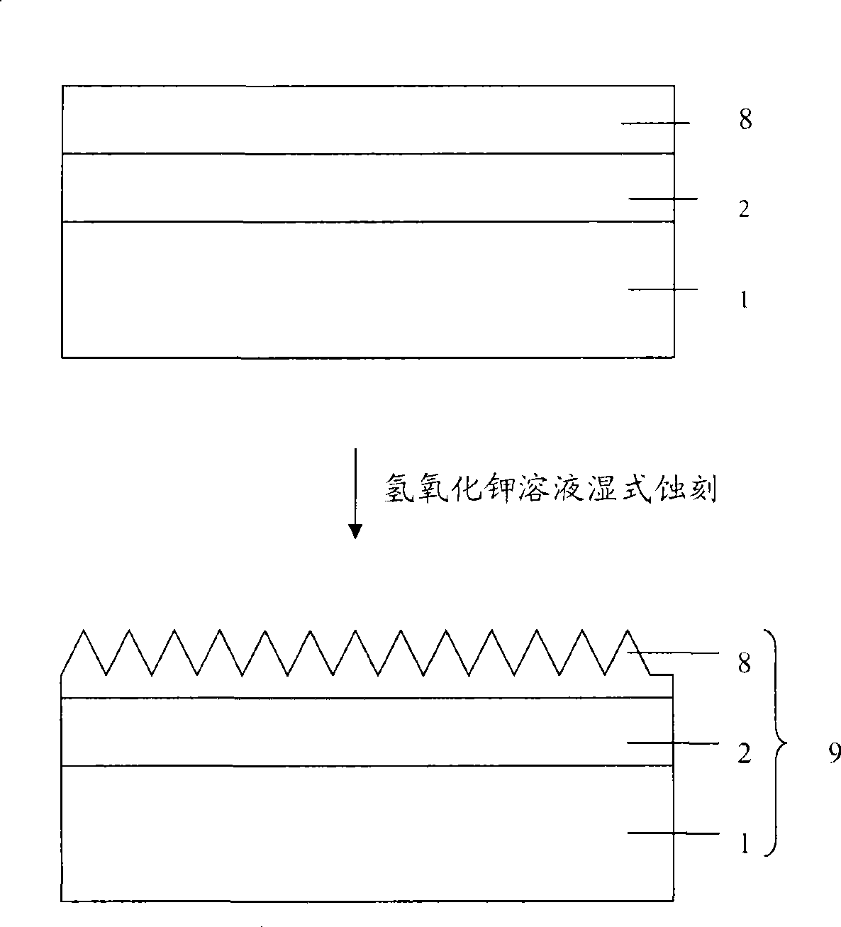
[0035] Such as image 3 As shown, a buffer layer 2 formed, for example, by undoped gallium nitride (u-GaN) is grown on an aluminum oxide (Sapphire) substrate 1 by metal organic chemical vapor deposition (MOCVD); a stamp layer 8, For example, it is undoped gallium nitride (u-GaN) or n-type doped gallium nitride (n-GaN), and the thickness of the stamp layer is at least 5000 Angstroms ( ). Next, after etching the stamp layer with 80°C potassium hydroxide (KOH) etching solution for 3 minutes, it has a zigzag (triangular) pattern, and its size is from 10nm to 1000nm, and the period is from 20nm to 2000nm. Die structure9.

Embodiment 3

[0037] another example Figure 4 As shown, a connection layer 13 formed, for example, by undoped gallium nitride is grown on an aluminum oxide (Sapphire) temporary substrate 14 by metalorganic chemical vapor deposition (MOCVD); an imprint layer 12 is, for example, undoped Heterogallium nitride or n-type doped gallium nitride, and the thickness of the stamp layer is at least 5000 angstroms ( ). Then use an electron gun (E-gun) or a concentrated plasma-assisted chemical vapor deposition system (Plasma-Enhanced Chemical Vapor Deposition, PECVD) to grow a buffer layer (bufferlayer) 11, such as metal or dielectric material; and then on the buffer layer The surface is bonded to a silicon substrate. Next, use laser lift off (Laser lift off) technology to remove the aluminum oxide temporary substrate 14, and then use an inductively coupled plasma ion etching system (Inductively Coupled Plasma Reactive IonEtching, ICP-RIE) to etch and remove the undoped gallium nitride formed connec...


PUM

PropertyMeasurementUnit
thicknessaaaaaaaaaa

Abstract

The invention discloses a die with a nano structure, comprising a substrate, a cushion layer arranged above the substrate and a die layer which is provided with the nano structure and is arranged above the cushion layer, wherein, the substrate is made of alumina or silicon, the cushion layer is made of gallium nitride, metal or dielectric materials, the die layer is made of materials not mixed with gallium nitride or n type gallium nitride. The invention also discloses a method for producing the die with the nano structure, comprising the following steps: forming the substrate; forming the cushion layer on the substrate; forming the die layer on the cushion layer, in addition, a nanoscale structure is formed on the upper surface of the die layer by adopting the organometallic chemical vapour deposition process or the potassium hydroxide solution wet-type etching method.

Description

technical field [0001] The invention relates to a nanometer stamp structure and its application on light-emitting elements. Background technique [0002] The luminous efficiency of solid-state light-emitting devices, such as light-emitting diodes, must be improved by increasing internal efficiency and light extraction efficiency, including improving the efficiency of the p-n junction (p-n junction) light-emitting layer, or using different substrates and various A crystal growth technology and other methods to improve the luminous efficiency. Further improvements are available with surface roughening. Because on the original flat surface, light rays within 17 degrees of incident angle can be taken out, but more than 17 degrees will be reflected back due to total reflection. If it is roughened, it can reduce the probability of total reflection and increase the light extraction rate. At present, the most effective method is to fabricate microstructures on the surface of the ...

Claims


Application Information

Patent Timeline
Patent Type & Authority Applications(China)
IPC IPC(8): G03F7/00H01L33/00
Inventor 姚久琳徐大正谢明勋
Owner EPISTAR CORP
Why Eureka
Try Eureka