Transversal epitaxial growth method for nano area of semiconductor film

A lateral epitaxial growth, semiconductor technology, applied in semiconductor/solid-state device manufacturing, nanotechnology, nanotechnology, etc., can solve the problems of uneven crystal quality, reduce the growth steps of lateral epitaxy technology, etc., and achieve the improvement of crystal quality and thin film crystal quality Uniform, diffusion-inhibiting effect

Inactive Publication Date: 2010-09-08
SUZHOU NANOJOIN PHOTONICS
View PDF0 Cites 1 Cited by
  • Summary
  • Abstract
  • Description
  • Claims
  • Application Information

AI Technical Summary

Problems solved by technology

[0006] The purpose of the present invention is to overcome the limitations of the above-mentioned prior art, solve the problem of uneven crystal quality when the traditional lateral epitaxy technology grows thin films, reduce the growth steps of the lateral epitaxy technology, so as to further improve the photoelectric characteristics of single crystal thin films

Method used


Image

  • Transversal epitaxial growth method for nano area of semiconductor film
  • Transversal epitaxial growth method for nano area of semiconductor film
  • Transversal epitaxial growth method for nano area of semiconductor film

Examples


Embodiment 1

[0035] Embodiment 1, referring to accompanying drawings 1 to 8, the nano-region lateral epitaxy technology adopted in the present invention includes the following steps:

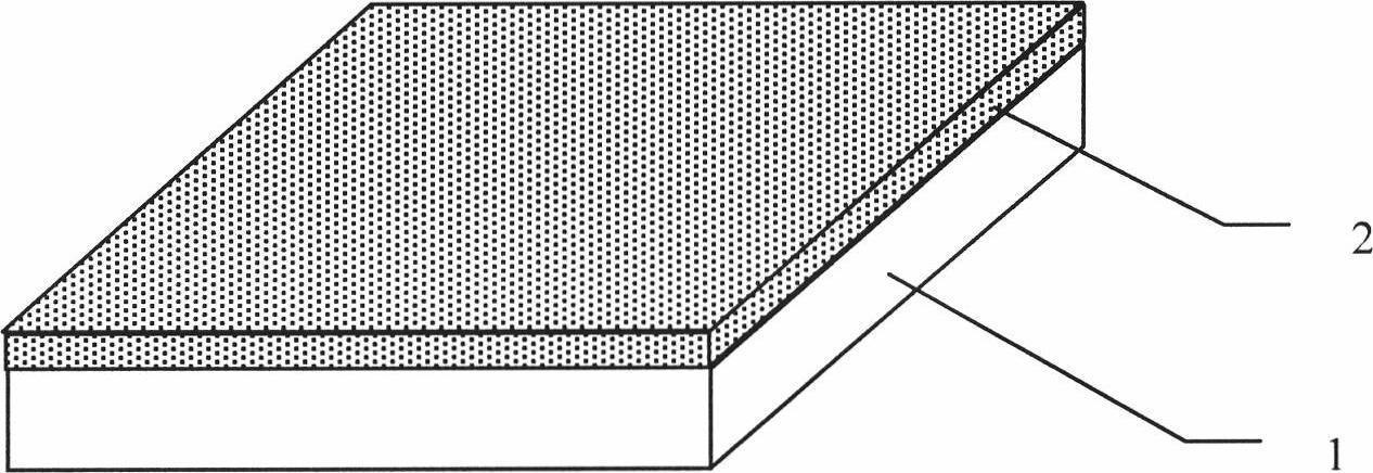
[0036] As shown in Figure 1, electron beam evaporation is used to vapor-deposit a thin layer of gold on the Si(111) substrate, and the thickness of the thin layer is 30nm;

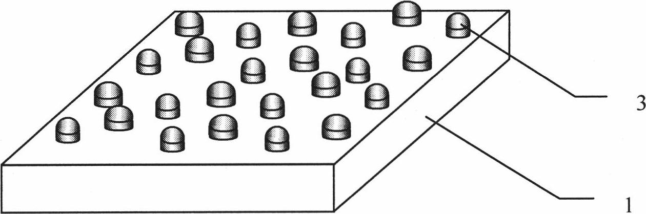
[0037] As shown in Figure 2, move into MOCVD, the pressure drops to 0.5atm, nitrogen gas is introduced, the temperature rises to 800°C and remains constant for 6 minutes, the gold thin layer is transformed into gold Au particles, the diameter of gold particles is 200-300nm, and the distribution density of metal particles is 10 9 / cm 2 , the duty cycle is 50%;

[0038] As shown in Figure 3, the pressure is reduced to 0.2atm, and hydrogen, trimethylgallium and ammonia are introduced for 2 minutes, and gallium nitride crystal nuclei are formed at the bottom of the gold particles, with a diameter of 200-300nm;

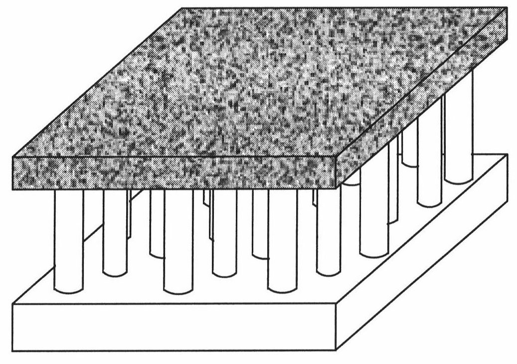
[0039] As shown in Figure 4...

Embodiment 2

[0043]Embodiment 2, referring to accompanying drawings 1 to 8, the nano-region lateral epitaxy technology adopted in the present invention includes the following steps:

[0044] As shown in Figure 1, a thin layer of platinum is evaporated on a Si(111) substrate by electron beam evaporation, and the thickness of the thin layer is 30nm;

[0045] As shown in Figure 2, move into MOCVD, the pressure drops to 0.5atm, nitrogen gas is introduced, the temperature rises to 800°C and remains constant for 6 minutes, the platinum thin layer is transformed into platinum Pt particles, the diameter of platinum particles is 200-300nm, and the distribution density of metal particles is 10 9 / cm 2 , the duty cycle is 50%;

[0046] As shown in Figure 3, the pressure is reduced to 0.3atm, and hydrogen, trimethylindium and ammonia are introduced for 2 minutes, and indium nitride crystal nuclei are formed at the bottom of platinum particles, with a diameter of 200-300nm;

[0047] As shown in Figur...


PUM

PropertyMeasurementUnit
thicknessaaaaaaaaaa
diameteraaaaaaaaaa
diameteraaaaaaaaaa

Abstract

The invention discloses a cross epitaxial growth method of a semiconductor film, which comprises the following steps: (1) a nucleated metallic catalyst film is evaporated on a substrate material and island-shaped metallic catalyst particles which are evenly distributed on the substrate are obtained after the film is annealed; (2) in external equipment, a crystal nucleus is formed on the bottom ofisland-shaped metallic particles; and then nano-column arrays grow longitudinally; (3) a wet etching method is used for eliminating the metallic catalyst on a nano-column to obtain semiconductor nano-column array structures with the same orientation and height; (4) the etched nano-column is put into the external equipment and a lateral epitaxy technology is used for integrating the nano-column arrays into a flat surface; and then a semiconductor epitaxial film with the required thickness grows on the flat surface. As cross epitaxy occurs in nano area, defects and diffusion of residual stress can be effectively restrained and the quality of film crystals is more uniform than that of film crystals prepared by the traditional method, thus improving the crystal quality of two-dimensional semiconductor films; furthermore, the invention has simple method and wide applicability.

Description

technical field [0001] The invention relates to a lateral epitaxial growth method of a semiconductor thin film, in particular to a method for vapor phase epitaxial growth of a high-quality gallium nitride single crystal thin film. Background technique [0002] Wide bandgap materials represented by GaN (gallium nitride) are the third-generation semiconductor materials after Si and GaAs, and are used to make electronic devices such as light-emitting diodes, lasers, detectors, high-frequency high-power transistors, etc. [0003] Since commercial high-quality bulk GaN crystals are not yet available, heterogeneous substrates are generally used for epitaxy. Unfortunately, there is a large lattice mismatch between GaN and sapphire substrates (or Si substrates). This leads to dislocations in the epitaxial layer, which will spread and pass through the entire epitaxial layer, limiting the improvement of GaN devices. In order to improve the quality of semiconductor thin films, a varie...

Claims


Application Information

Patent Timeline
Patent Type & Authority Patents(China)
IPC IPC(8): H01L21/205C23C16/44B82B3/00
Inventor 王怀兵黄小辉杨辉张书明
Owner SUZHOU NANOJOIN PHOTONICS
Why Eureka
Try Eureka