Preparation method for molybdenum disulfide nanometer film with preset patterns

A technology of molybdenum disulfide and nano-film, which is applied in the manufacture of semiconductor/solid-state devices, electrical components, circuits, etc., can solve the problems of time-consuming and laborious, damage or pollution of molybdenum disulfide film, and achieve the effect of uniform crystal quality

Inactive Publication Date: 2016-07-06
GENERAL RESEARCH INSTITUTE FOR NONFERROUS METALS BEIJNG
View PDF7 Cites 11 Cited by
  • Summary
  • Abstract
  • Description
  • Claims
  • Application Information

AI Technical Summary

Problems solved by technology

In the past, when making molybdenum disulfide devices, the method of ion etching the prepared molybdenum disulfide film was usually used to obtain the desired shape. This method was time-consuming and laborious, and the molybdenum disulfide film was easily damaged during the etching process. or pollution

Method used


Image

  • Preparation method for molybdenum disulfide nanometer film with preset patterns
  • Preparation method for molybdenum disulfide nanometer film with preset patterns

Examples


preparation example Construction

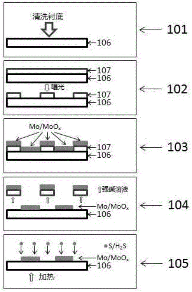
[0030] figure 1 The process flow of the method for preparing the molybdenum disulfide film with preset graphics in the present invention includes:

[0031] Step 101: Cleaning the substrate. The substrate can be a silicon substrate, a germanium substrate, a silicon carbide substrate, a sapphire substrate, etc., which mainly serve as a support for the precursor and the molybdenum disulfide sample generated later;

[0032] Step 102: Spin-coat a layer of photoresist on the substrate with a coater (it can be glue for ultraviolet exposure, ion beam exposure, and electron beam exposure, etc., depending on the specific process requirements), and use a mask with a corresponding pattern The film plate exposes and develops the substrate coated with photoresist, and removes the photoresist at the preset pattern part;

[0033] Step 103: Deposit a layer of metal molybdenum film or molybdenum oxide film on the substrate by using magnetron sputtering technology, electron beam evaporation or ...

Embodiment 1

[0038] A kind of molybdenum disulfide CVD preparation method that can preset pattern, comprises following specific steps:

[0039] Step 101: Cleaning the substrate. The substrate is a thermally oxidized silicon substrate, which mainly serves as a support for the precursor and the later-generated molybdenum disulfide sample.

[0040] Step 102: Spin-coat a layer of photoresist positive resist on the clean silicon substrate with a coater, use a mask plate to expose the pre-baked sample, and develop the sample after post-baking;

[0041] Step 103: using a magnetron sputtering device to deposit a layer of metal molybdenum as a precursor on the sample substrate. The process parameters used in the sputtering process were argon gas flow rate of 20 sccm, sputtering pressure of 2.0 Pa, sputtering power of 10 W, and sputtering time of 1 min. The thickness of the obtained molybdenum film is about 5nm;

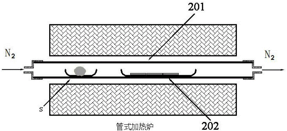
[0042] Step 104: Soak the sample coated with molybdenum film in acetone solvent for ...


PUM


Abstract

The invention belongs to the technical field of semiconducting material and especially relates to a preparation method for a molybdenum disulfide nanometer film with preset patterns. The method comprises following steps: (1) presetting patterns on a substrate; (2) depositing a molybdenum-source film on the substrate with preset patterns through a film deposition method; (3) removing photo-resist by use of ketone solvent; (4) preparing the molybdenum disulfide film with preset patterns by means of the chemical vapor deposition (CVD) method. By means of the method, a uniform molybdenum disulfide film with preset patterns is obtained, and the possibility that the film may be damaged or polluted due to later shape processing to the molybdenum disulfide film is reduced.

Description

technical field [0001] The invention belongs to the technical field of semiconductor materials, in particular to a method for preparing a molybdenum disulfide nanometer film with preset patterns. Background technique [0002] Molybdenum disulfide has high transmittance and theoretical mobility, and has a band gap of 1.2eV to 1.8eV. The theoretical switch ratio of FET using molybdenum disulfide as the channel material can reach 10 10 , has a very broad application prospect in the field of electronic devices. In the application of sensors, the band gap of the molybdenum disulfide layer can change with the change of the pH value or humidity of the surrounding environment, so it can be used as a sensor material; in flexible and transparent electronic devices, molybdenum disulfide can be used as Transparent channel material; in addition, molybdenum disulfide also has certain advantages in terms of physical properties, and its Young's modulus is as high as 0.33TPa±0.07TPa, which ...

Claims


Application Information

Patent Timeline
Patent Type & Authority Applications(China)
IPC IPC(8): H01L21/365H01L21/027
Inventor 史志天魏峰赵鸿滨张艳
Owner GENERAL RESEARCH INSTITUTE FOR NONFERROUS METALS BEIJNG
Why Eureka
Try Eureka