A ZnS monocrystal nanowire growing method
A technology of single crystal nanometer and catalyst, which is applied in the direction of single crystal growth, crystal growth, single crystal growth, etc., to achieve the effect of simple method, uniform shape and easy promotion
- Summary
- Abstract
- Description
- Claims
- Application Information
AI Technical Summary
Problems solved by technology
Method used
Image
Examples
Embodiment 1
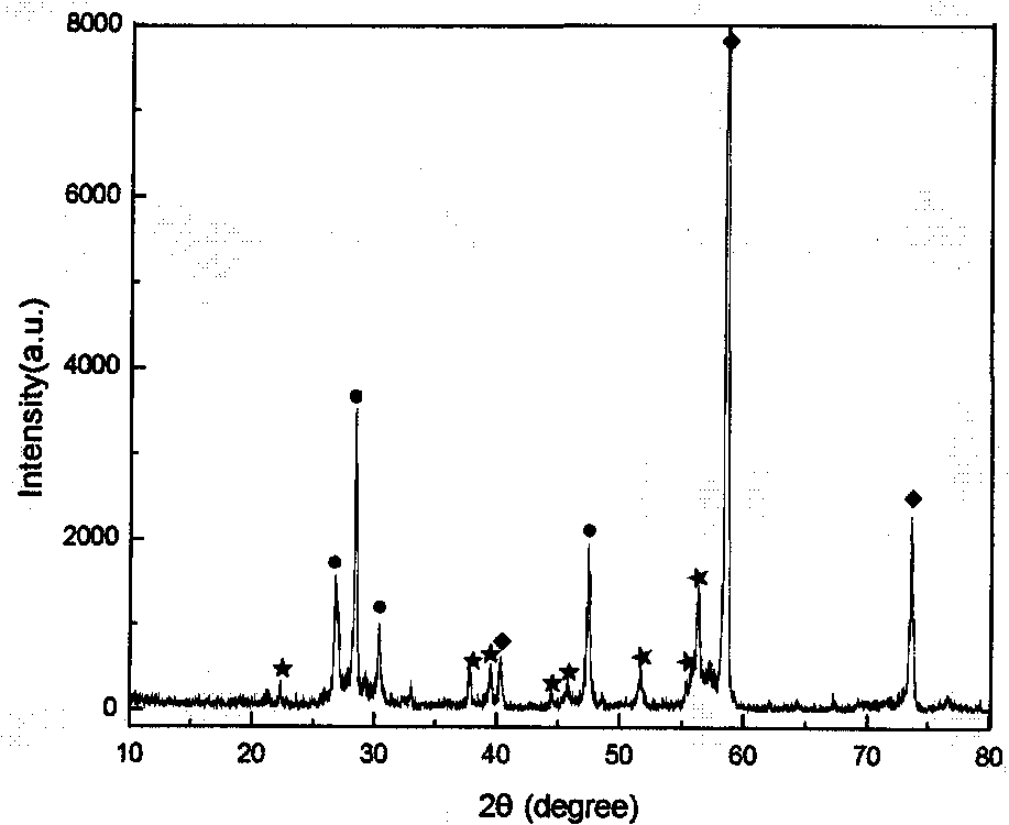
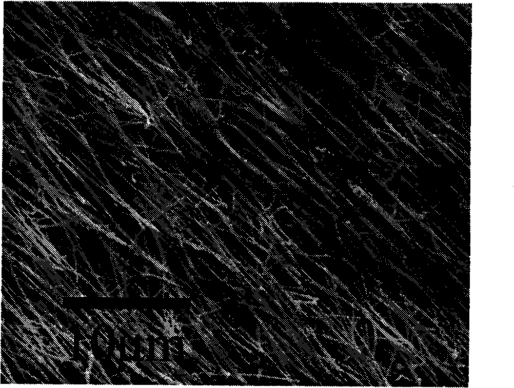
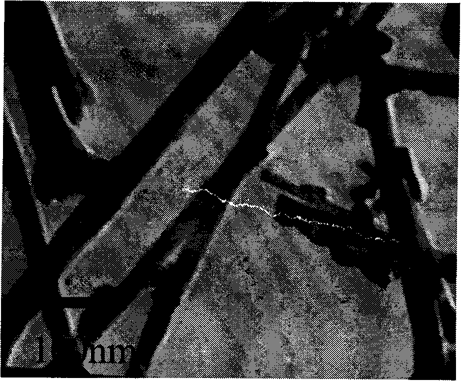
[0024] Use high-purity ZnS powder (99.5%) as raw material and high-purity Bi powder as catalyst. After the two are uniformly mixed at 1mol:0.015mol, the powder is placed on the molybdenum sheet heater, and the molybdenum sheet is selected as the substrate for evaporation. About 2.0cm above the source, seal the evaporation chamber, when the vacuum reaches 1.4×10 -2 After Pa, the current was gradually increased to 130A at a rate of 3.3A / min and kept for 5 minutes. There are off-white deposits on the substrate surface. The scanning electron microscope image shows that the surface morphology of the substrate deposit is a nanowire with a diameter of 80-100nm and a line length of 10-15μm, such as figure 2 . Its transmission electron microscope picture is as follows image 3 , high-resolution transmission electron microscope pictures such as Figure 4 , it can be seen that it is a single crystal. XRD analysis results show that the main phase of the product is hexagonal ZnS, and...
Embodiment 2
[0026] High-purity ZnS powder (99.5%) is used as raw material, high-purity Bi powder is used as catalyst, the two are evenly mixed according to the ratio of 1mol:0.005mol, and the powder is placed on the molybdenum sheet heater, and the molybdenum sheet is placed on the substrate as the substrate. About 2.0cm above the evaporation source. When the vacuum reaches 2.4×10 -2 After Pa, the evaporation chamber was sealed, and the current was gradually increased to 130 A at a current increase rate of 3.3 A / min and then kept for 10 minutes. There are white deposits on the substrate surface. The surface morphology of the substrate deposit observed by SEM is a single crystal nanowire with a length of 10-20 μm and a diameter of 100-150 nm, such as Figure 5 .
Embodiment 3
[0028] Use high-purity ZnS powder (99.5%) as raw material, high-purity Sn powder as catalyst, and after the two are evenly mixed according to the ratio of 1mol:0.025mol, the powder is placed on the molybdenum sheet heater, and the molybdenum sheet is used as the substrate. About 1.5cm above the evaporation source. When the vacuum reaches 8.0×10 -3 After Pa, the evaporation chamber was sealed, and the current was gradually increased to 130 A at a current increase rate of 3.3 A / min and then kept for 10 minutes. A white deposit was obtained on the molybdenum substrate. The surface morphology of the deposit observed by SEM is uniformly distributed nanowires with a length of 10-20 μm and a diameter of 150-200 nm, such as Image 6 .
PUM
 Abstract
Description
Claims
Application Information


