Semiconductor electronic component and semiconductor device using the same
A technology of electronic components and semiconductors, applied in the direction of semiconductor devices, electrical components, electric solid devices, etc., can solve the problems of inability to wire bond, pollute external electrodes, etc., and achieve the effect of increasing the amount of information
- Summary
- Abstract
- Description
- Claims
- Application Information
AI Technical Summary
Problems solved by technology
Method used
Image

Examples
no. 1 approach
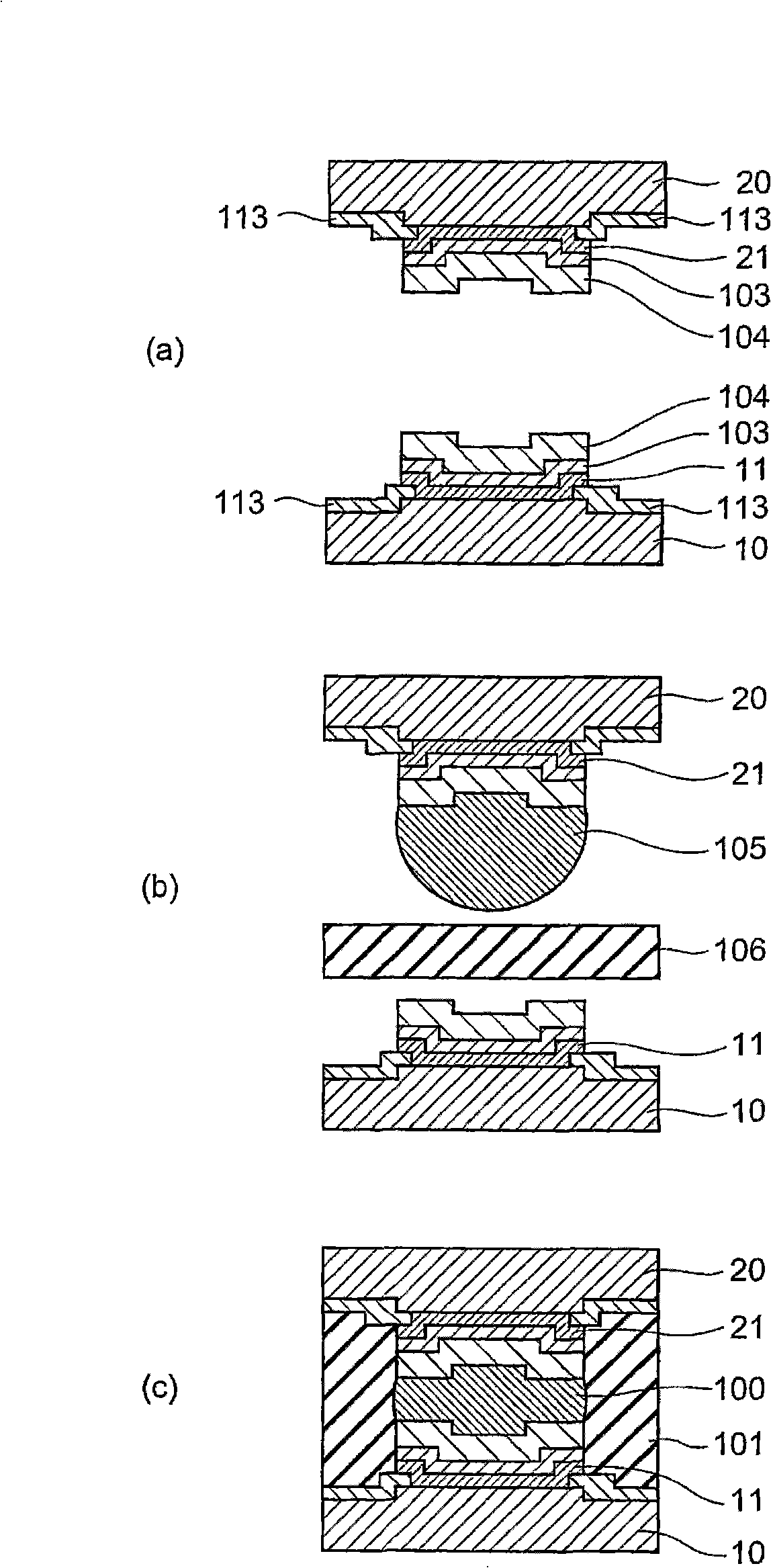
[0105] First, refer to image 3 , the method of manufacturing the semiconductor electronic component according to the first embodiment of the present invention will be described.
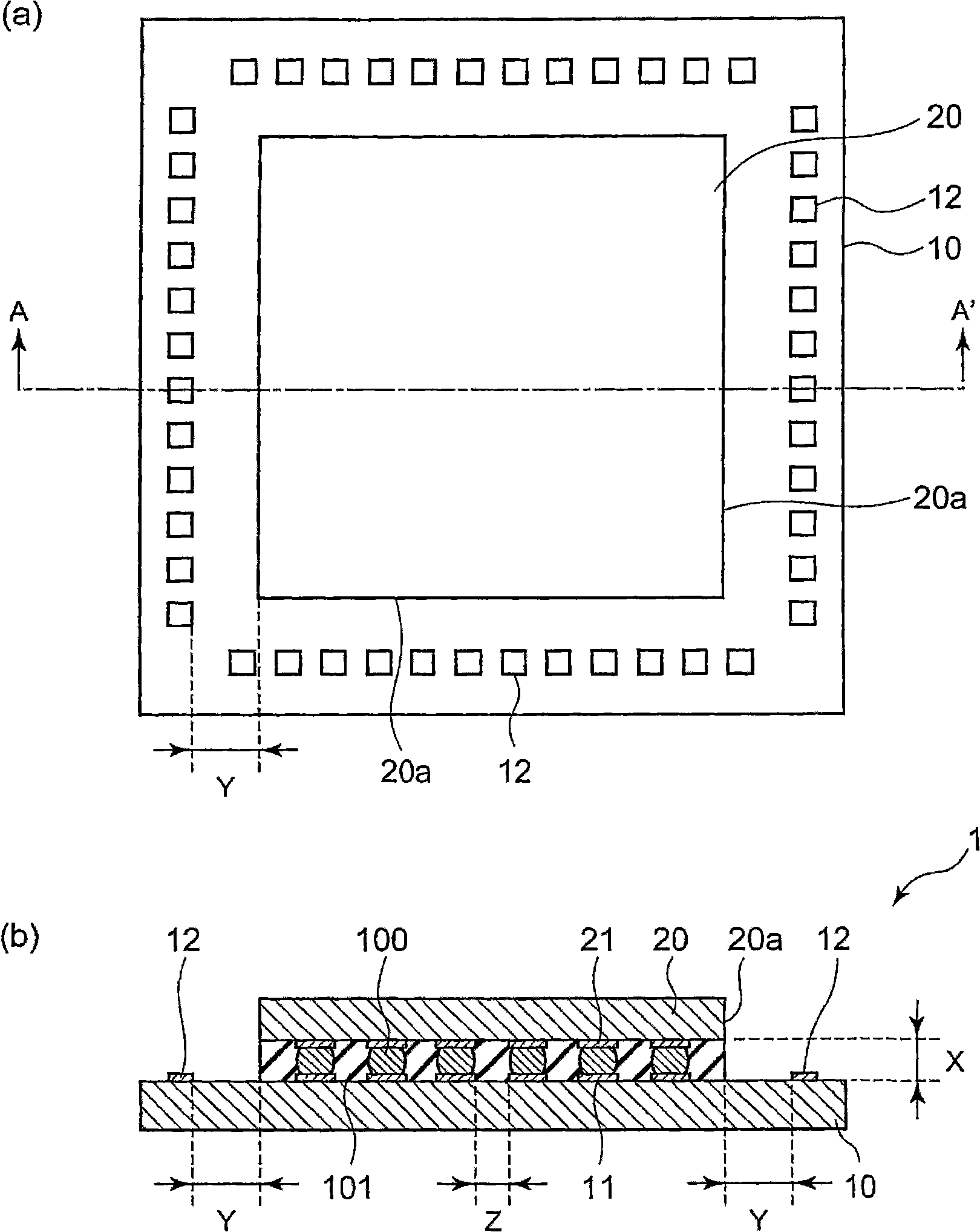
[0106] Such as image 3 As shown in (a), first, the semiconductor chip 10 provided with the internal electrode 11 in the circuit surface and the semiconductor chip 20 provided with the internal electrode 21 in the circuit surface are prepared. In order to improve the electrical connectivity, the surfaces of the internal electrodes 11 and 21 may be preliminarily subjected to treatments such as cleaning, polishing, plating, and surface activation. For example, if image 3 As shown in (a), UBM (under barrier metal buried metal) layers 103 and 104 may be formed on the surfaces of internal electrodes 11 and 21 using Ti, Ti / Cu, Cu, Ni, Cr / Ni, or the like. The UBM layer can be single layer or multilayer. In addition, on the surfaces of the semiconductor chips 10 and 20, in order to protect the semicond...
no. 2 approach
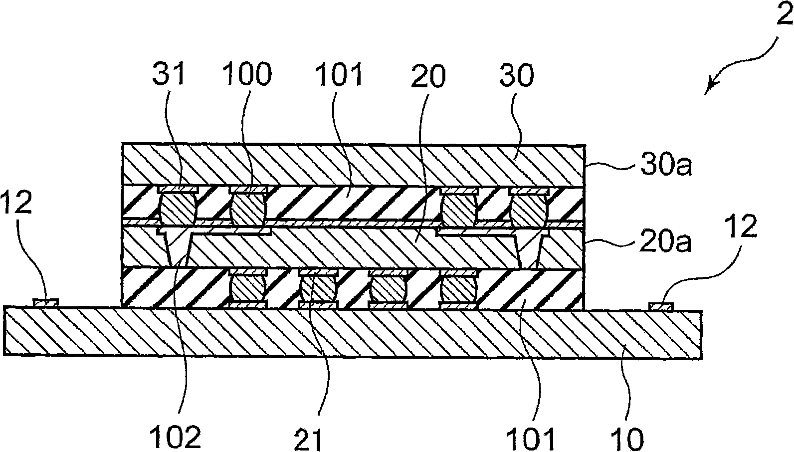
[0196] Next, refer to Figure 4 , a method of manufacturing a semiconductor electronic component according to a second embodiment of the present invention will be described.
[0197] Such as Figure 4 As shown in (a), the semiconductor chip 10 provided with the internal electrodes 11 and the semiconductor chip 20 provided with the internal electrodes 21 are arranged so that the surface (circuit surface) provided with the internal electrodes faces each other.
[0198] The protective film 107 may be formed on the surfaces of the semiconductor chip 10 and the semiconductor chip 20 so that the internal electrodes 11 and 21 are opened, respectively. For example, a protective film of an organic resin such as a polyimide film, a polybenzoxazole film, or a polybenzocyclobutene film can be formed. Thereby, the solder component can be easily guided between the opposing internal electrodes, and the electrical connection between the internal electrodes can be improved. In addition, it ...
Embodiment 1、2
[0265] First, a thermal oxide film 114 with a thickness of 0.4 μm is formed on the entire circuit surface of the semiconductor chip 10 , 20 . Next, Al / 0.5Cu was sputtered to a thickness of 0.4 μm as a metal layer, and wirings other than necessary portions were dry-etched using a resist film to form internal electrodes 11 and 21 . After removing the mask, a SiN film (passivation film) 113 with a thickness of 0.2 μm was formed on the entire surface by CVD, and further, the metal layer portion (internal electrode surface) was soft etched using a resist film. Next, a polyimide layer with a thickness of 3 μm was applied and developed to partially open the metal layer, and then the polyimide layer was cured to form a stress relaxation layer (protective film) 107 . Next, sputtering was performed in the order of 0.05 μm thick Ti and 1 μm thick Cu to form UBM layers 103 and 104 . Thereby, connection pads (pad size: 60 μm square; inter-pad distance: 40 μm; pad pitch: 100 μm) were forme...
PUM
| Property | Measurement | Unit |
|---|---|---|
| Softening point | aaaaa | aaaaa |
| Melt viscosity | aaaaa | aaaaa |
| Melting point | aaaaa | aaaaa |
Abstract
Description
Claims
Application Information