Method for etching matte on surface of single crystal silicon solar energy battery
A solar cell, monocrystalline silicon technology, applied in circuits, electrical components, climate sustainability, etc., can solve the problems of high surface reflectivity of silicon wafers, expensive IPA, large pyramid particles, etc., to achieve uniform distribution and tight arrangement , the effect of reducing reflectivity
- Summary
- Abstract
- Description
- Claims
- Application Information
AI Technical Summary
Problems solved by technology
Method used
Image
Examples
Embodiment 1
[0022] Clean the P-type crystal plane Czochralski single crystal silicon wafer with a resistivity of 1Ωcm by conventional methods, and then put the silicon wafer into a sodium hypochlorite (NaClO) solution with a concentration of 10wt% at a temperature of 85±1°C for etching 25 minutes to remove the silicon surface damage layer. Then put the corroded silicon chip into 80±1°C texturing solution (sodium hypochlorite 5wt%, ethanol 10vl%), react for 5-10 minutes, take out the silicon chip, clean it with deionized water, and dry it.
Embodiment 2
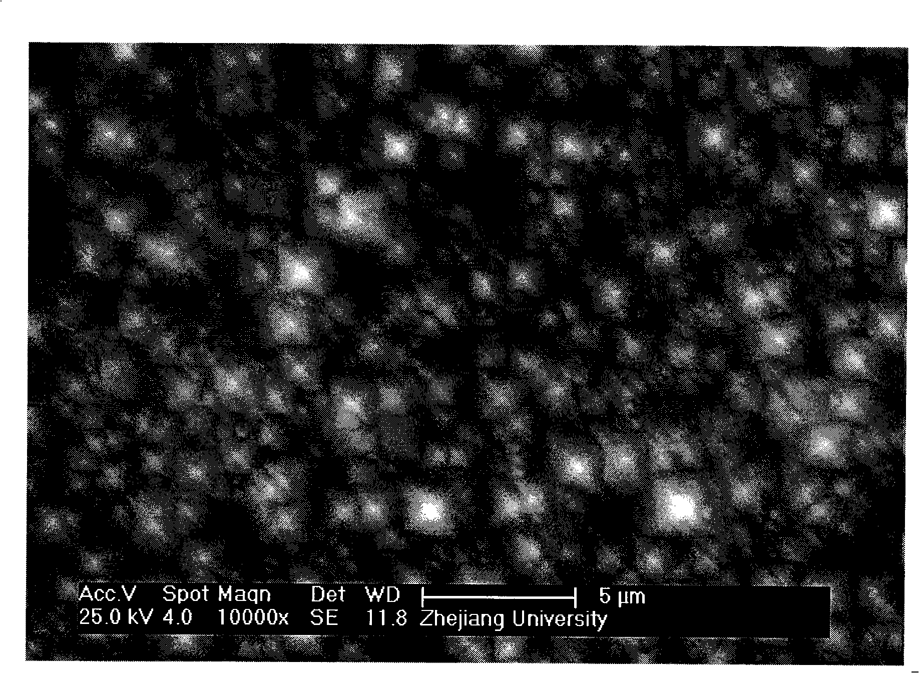
[0024] According to the method of Example 1, the silicon wafer was put into the etching solution to remove the damaged surface layer. The proportion of the etching solution was 15 wt% sodium hypochlorite, the temperature was controlled at 85±1° C., and the reaction time was 30 minutes. The corroded silicon chip is put into the texturing solution composed of 5wt% sodium hypochlorite, 10vl% ethanol and deionized water. The reaction time is 15 minutes, and the temperature is controlled at 80±1°C. Finally, the wafers were rinsed with deionized water and dried. Such as figure 1 As shown, under the scanning electron microscope, it can be seen that a dense pyramid structure is formed on the surface of the silicon wafer, and the size of the pyramid particles is about 1-4 μm, and the distribution is uniform and the coverage rate is high.
Embodiment 3
[0025] Embodiment 3 (comparative example)
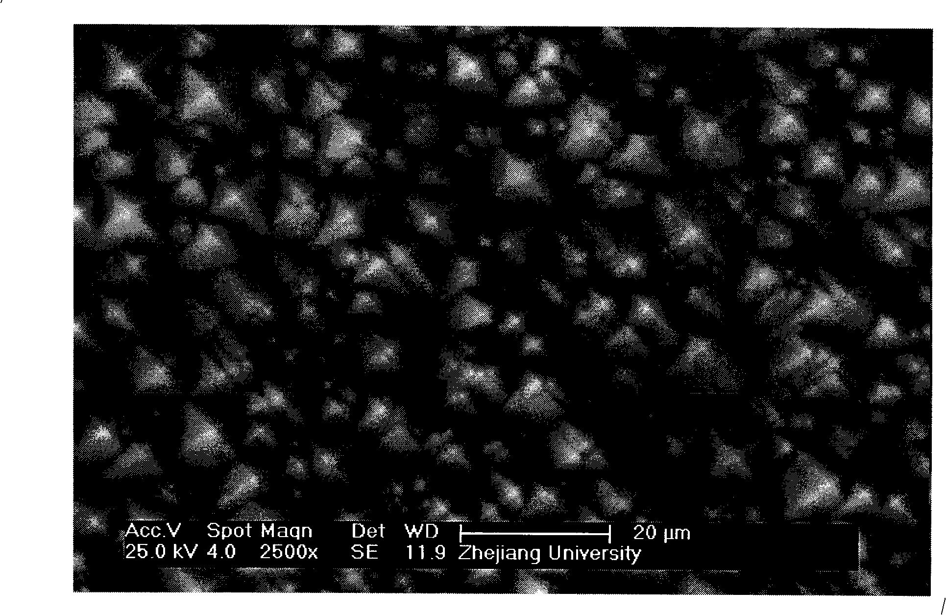
[0026] This solution uses a conventional corrosion solution, its components are: sodium hydroxide, ethanol and deionized water, the respective percentages are NaOH2wt%, CH3COOH 10vl%. Clean the P-type crystal plane Czochralski silicon wafer with a resistivity of 1Ωcm by conventional methods, and then put it into a sodium hydroxide (NaOH) solution with a temperature of 85±1°C and a concentration of 15wt% for 10 minutes to remove the surface damage layer. Then put the corroded silicon chip into the prepared etching solution, texture it at 80±1°C for 15 minutes, take out the textured silicon chip, wash it with deionized water, and dry it. Such as figure 2 As shown, under the scanning electron microscope, it can be seen that the pyramid structure formed on the surface of the silicon wafer is relatively large in shape.
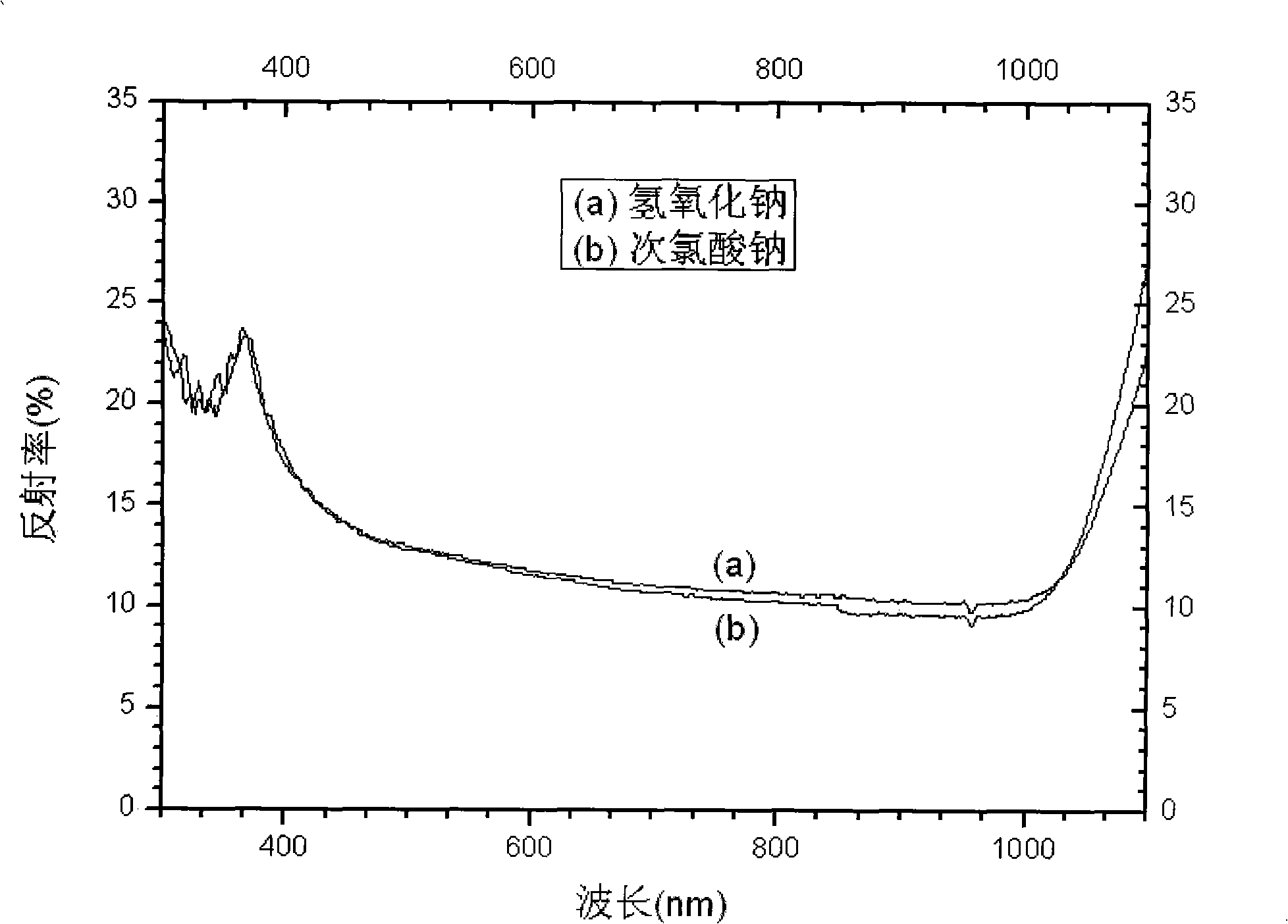
[0027] The main technical performance indicators of the texturing reagent of the present invention are shown in Ta...
PUM
 Abstract
Description
Claims
Application Information


