Nitride luminescent device and production method thereof

A technology of light-emitting devices and nitrides, applied in semiconductor devices, electrical components, circuits, etc., can solve the problems of sharp drop in efficiency of high-output power LEDs, increase in electron leakage probability, and reduce external quantum efficiency, and improve carrier distribution. Non-uniformity, reduction of electron leakage, favorable effect of transport

Inactive Publication Date: 2009-09-23
XIAMEN UNIV
View PDF0 Cites 53 Cited by
  • Summary
  • Abstract
  • Description
  • Claims
  • Application Information

AI Technical Summary

Problems solved by technology

As the injection current increases, it will inevitably lead to a large number of carriers in the quantum well close to the p region, which will increase the probability of electron leakage from the active region, thereby greatly reducing the external quantum efficiency of the active region, which also leads to high output. The main reason for the sudden drop in power LED efficiency (X.F.Ni, Q.Fan, R.Shimada, et al., Reduction of efficiency droop in InGaN light emitting diodes by coupled quantum wells, 2008, 93(17): 171113; J.Q.Xie, X.F. Ni, Q.Fan, et al., On the efficiency droop in InGaN multiple quantum well blue light emitting diodes and its reduction with p-doped quantum well barriers, ApplPhys Lett, 2008, 93(12): 121107)
At the same time, due to the enhanced band filling effect, the emission wavelength will also undergo a significant blue shift.

Method used


Image

  • Nitride luminescent device and production method thereof
  • Nitride luminescent device and production method thereof
  • Nitride luminescent device and production method thereof

Examples


Embodiment Construction

[0031] In order to make the object, technical solution and advantages of the present invention clearer, the present invention will be described in further detail below in conjunction with specific embodiments and with reference to the accompanying drawings.

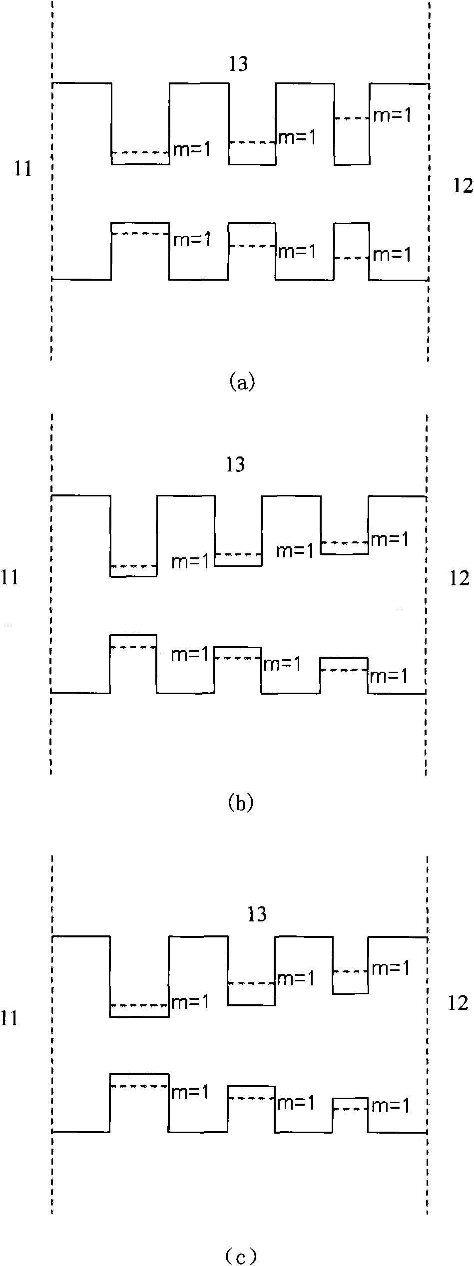
[0032] figure 1 It is a schematic diagram of the energy band of an asymmetrically coupled quantum well active region; the active region includes at least 2 quantum wells (take 3 as an example in the figure), and the barrier layer of each group of quantum wells is very thin (<10nm), so as to realize efficient tunneling of carriers. The energy band structure of the quantum well mainly has the following three forms: (a) It is an asymmetrically coupled quantum well with different well widths, and the width of the quantum well decreases sequentially from the n-type electron injection layer to the p-type hole injection layer; (b) is an asymmetrically coupled quantum well with different components, and the In content of the qua...


PUM


Abstract

The invention discloses a nitride luminescent device and a production method thereof, which relate to a semiconductor luminescent device and provide a nitride luminescent device with an asymmetric coupled multi-quantum well structure being the active area. The device at least comprises an n-type electron injection layer, a p-type hole injection layer and a multi-quantum well active layer which is sandwiched between the n-type electron injection layer and the p-type hole injection layer, and the active layer is composed of asymmetric coupled quantum well structures. The barrier layer of the quantum well is thinner, thus being easy to realize the tunneling of current carriers; transition energy between ground-state energy level in the quantum wells is gradually changed; the quantum wells with high transition energy are close to the p-type hole injection layer; and the quantum wells with low transition energy are close to the n-type electron injection layer. The active area structure can enhance the tunneling transportation of the holes in the quantum well active area, simultaneously block the tunneling transportation of electrons in the quantum well active area, improve the uneven distribution of current carriers in the active area of the nitride luminescent device, reduce electron leakage and energy band filling effect, and realize high-efficiency luminescence.

Description

technical field [0001] The present invention relates to a semiconductor light-emitting device, in particular to a nitride light-emitting device in which an asymmetrically coupled quantum well is an active region, such as a light-emitting diode (LED) or a laser diode (LD). Background technique [0002] GaN-based materials refer to GaN, InN, AlN and their ternary and quaternary compounds. They are direct band gap semiconductor materials with excellent mechanical and chemical properties. At room temperature, their emission wavelengths cover near-infrared, visible and deep ultraviolet bands. . Semiconductor light-emitting devices based on GaN-based materials have broad application prospects in the fields of large-screen full-color display, lighting, information storage, and medicine. [0003] At present, nitride light-emitting devices mainly use a multi-quantum well structure as the active layer, and the carrier injection method is bipolar input, that is, electrons and holes ar...

Claims


Application Information

Patent Timeline
Patent Type & Authority Applications(China)
IPC IPC(8): H01L33/00H01S5/34
Inventor 张江勇张保平王启明蔡丽娥余金中
Owner XIAMEN UNIV
Why Eureka
Try Eureka