Method for designing and extending 808nm laser material by adopting (In)GaAs/GaAs straining isolated layer

A technology for isolation layers and lasers, applied to lasers, laser components, semiconductor lasers, etc., can solve problems such as the decline in output power slope efficiency, and achieve the effects of improving performance, improving overall performance, quantum efficiency and high temperature characteristics

Inactive Publication Date: 2009-11-04
CHANGCHUN UNIV OF SCI & TECH
View PDF0 Cites 7 Cited by
  • Summary
  • Abstract
  • Description
  • Claims
  • Application Information

AI Technical Summary

Problems solved by technology

The continuous output power of the device is 2W at room temperature, and at 95°C, the output power can reach 500mW under continuous operation, and the output power slope efficiency drops by 23%.

Method used


Image

  • Method for designing and extending 808nm laser material by adopting (In)GaAs/GaAs straining isolated layer

Examples


Embodiment Construction

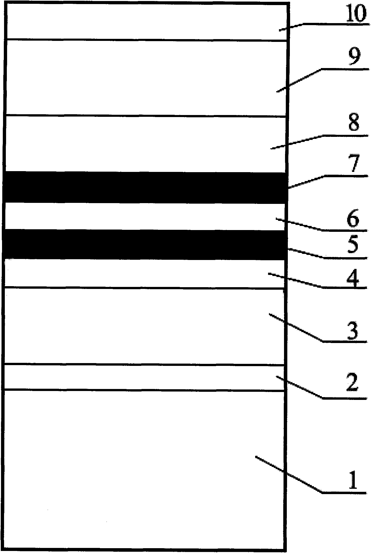
[0012] Such as figure 1 As shown, a structure of an 808nm semiconductor laser material that uses (In)GaAs / GaAs strain isolation layer to efficiently realize high efficiency and high temperature operation includes:

[0013] The substrate (1) has a (100) orientation and a Si doping concentration of 1 to 2×10 18 cm -3 GaAs crystal material, EPD≤100 -2 ; GaAs buffer layer (2), growth temperature 580 ° C, n (Si) doped 2 × 10 18 cm -3 , with a thickness of 1 μm thick;

[0014] Al 0.55 Ga 0.45 As lower cladding layer (3), n(Si) doped 3.0×10 17 cm -3 , 1.2 μm thick;

[0015] Al 0.4 Ga 0.6 As lower waveguide layer (4), 0.35 μm thick;

[0016] Introduce a layer of (In)GaAs / GaAs strain isolation layer (5) with 1 to 2 periods to increase the physical distance between the quantum well and the growth interface of the initial barrier layer and strengthen the reflection of electrons, and reduce the active area Accumulation of oxygen at the heterojunction interface with the wavegu...


PUM


Abstract

High power 808nm semiconductor laser is widely applied to pumping Nd:YAG solid laser, laser processing, laser medical treatment and other fields, due to the fact that the semi-conductor laser has the advantages of high efficiency, compact structure, convenient modulation and the like. Meanwhile, people always concern the problems of the semi-conductor laser on efficiency, temperature property and the like. The invention provides design and extension growth of a 808nm laser material by adopting (In)GaAs/GaAs straining isolated layer. Adopting insertion of strained quantum barrier into a wave guide layer and an active layer as a method for improving the physical distance between a quantum well and a growth interface of an initial barrier layer and the electron reflecting layer, and reducing accumulation of heterojunction interface oxygen of an active region and a wave guide region; multiple effective methods and special wave guide structure designs are utilized in the extension growth to improve conduction band edge potential energy, enhance capability of preventing current carrier leakage, restrict current density of threshold, and improve temperature property and quantum efficiency of the laser.

Description

technical field [0001] The invention relates to the technical field of semiconductor laser materials, and belongs to the technical fields of semiconductor laser structure design and material epitaxial growth. Background technique [0002] High-power 808nm semiconductor lasers are widely used in the fields of pumping Nd:YAG solid-state lasers, laser processing and laser medical treatment. This is because semiconductor lasers have the advantages of high efficiency, compact structure, and convenient modulation. But at the same time, people have been paying attention to issues such as the efficiency and temperature characteristics of semiconductor lasers. [0003] Due to the particularity of the energy band structure of semiconductor lasers, the emission wavelength of interband transition type (bipolar) semiconductor lasers is a function of the forbidden band width of the bulk material and the material parameters (quantum size, doping) in the quantum well structure, so The las...

Claims


Application Information

Patent Timeline
Patent Type & Authority Applications(China)
IPC IPC(8): H01S5/343H01S5/20H01S5/028
Inventor 刘国军李占国李林李梅尤明慧芦鹏陈佳音李辉王勇乔忠良邓昀高欣
Owner CHANGCHUN UNIV OF SCI & TECH
Why Eureka
Try Eureka