Resistance transition type memory and manufacturing method thereof

A technology of resistance conversion and manufacturing method, which is applied in the field of information storage, can solve the problems of high operating voltage of Flash memory devices, insufficient device retention time, and insufficient durability, etc., and achieves the effects of simple structure, low cost, and reduced operating voltage

Inactive Publication Date: 2009-11-11
INST OF MICROELECTRONICS CHINESE ACAD OF SCI
View PDF0 Cites 16 Cited by
  • Summary
  • Abstract
  • Description
  • Claims
  • Application Information

AI Technical Summary

Problems solved by technology

However, Flash memory devices have disadvantages such as excessive operating voltage, slow operating speed, insufficient endurance, and too thin a tunneling dielectric layer in the process of device size reduction, which will lead to insufficient device retention time.
This limits the further development of traditional Flash memory to a certain extent

Method used


Image

  • Resistance transition type memory and manufacturing method thereof
  • Resistance transition type memory and manufacturing method thereof
  • Resistance transition type memory and manufacturing method thereof

Examples


Embodiment 1

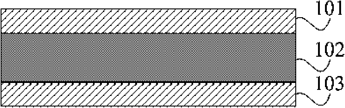
[0030] Figure 4 It is a schematic diagram of the basic structure of the resistance transition memory according to the embodiment of the present invention. Such as Figure 4 As shown, the resistance transition memory includes a substrate 401, a lower electrode 402 disposed on the substrate 401, a resistance transition memory layer 403 disposed on the lower electrode 402, and an upper electrode disposed on the resistance transition memory layer 403 404.

[0031] The substrate 401 is generally made of silicon dioxide, doped silicon dioxide or other insulating materials.

[0032] Both the lower electrode 402 and the upper electrode 404 are made of materials with a work function of 4.5 eV-6 eV. The lower electrode 402 and the upper electrode 404 can be single-layer metal electrodes formed of metals such as Au, Co, Ir, Re, Pd or Pt, or metal alloys such as Ti-Pt, Co-Ni or Pt-Hf. Double-layer metal electrodes can also be made of other conductive materials with higher work functi...

Embodiment 2

[0036] Figure 5 It is a flowchart of a fabrication method of a resistance transition memory according to an embodiment of the present invention. Such as Figure 5 Shown, described preparation method comprises the following steps:

[0037] Step 501: forming a bottom electrode with a work function of 4.5 eV-6 eV on the substrate.

[0038] The lower electrode can be formed by physical vapor deposition or chemical vapor deposition such as electron beam evaporation and sputtering.

[0039] Step 502: forming a P-type semiconductor binary metal oxide film on the lower electrode as a resistance switching storage layer.

[0040] The resistance switching storage layer can be formed by electron beam evaporation, plasma enhanced chemical vapor deposition (PECVD) or atomic layer deposition (ALD).

[0041] Step 503: forming an upper electrode with a work function of 4.5 eV-6 eV on the resistance transition storage layer.

[0042] The upper electrode can be formed by physical vapor dep...


PUM


Abstract

The invention relates to a resistance transition type memory and a manufacturing method thereof, belonging to the technical field of information storage. The memory comprises an upper electrode, a lower electrode and a resistance transition storage layer positioned between the upper electrode and the lower electrode, wherein, the upper electrode and the lower electrode are both made of materials with work function of 4.5-6 electron volts, and the resistance transition storage layer is a thin film made of P-type semiconductor binary metal oxides. The resistance transition type memory of the invention has simple structure, employs the materials with high work function to manufacture the upper electrode and the lower electrode, and uses the thin film made of the P-type semiconductor binary metal oxides as the resistance transition storage layer so that interfaces of the upper electrode, the lower electrode resistance transition storage layer can form ohmic contact or low Schottky contact and a memory device can realize the transition between high resistance state and low resistance state under low operating voltage, thus reducing the operating voltage of the memory device.

Description

technical field [0001] The invention relates to a memory and a manufacturing method thereof, in particular to a resistance transition type memory and a manufacturing method thereof, belonging to the technical field of information storage. Background technique [0002] With the increasing popularity of portable personal devices such as mobile phones, MP3, MP4, and notebook computers, non-volatile memory plays an increasingly important role in the semiconductor industry. Its biggest advantage is that the stored data remains Can be kept for a long time, it not only has the characteristics of ROM, but also has a high access speed. At present, flash memory (Flash) is still the mainstream of the non-volatile memory in the market. With the rapid development of digital high-tech, higher requirements are placed on the performance of memory, such as high speed, high density, low power consumption, long life and smaller size. However, Flash memory devices have disadvantages such as e...

Claims


Application Information

Patent Timeline
Patent Type & Authority Applications(China)
IPC IPC(8): H01L45/00G11C11/56
Inventor 刘明李颖弢龙世兵王琴刘琦张森王艳左青云
Owner INST OF MICROELECTRONICS CHINESE ACAD OF SCI
Why Eureka
Try Eureka