Ex-situ doped semiconductor transport layer

A semiconductor and external doping technology, applied in semiconductor/solid-state device manufacturing, electrical components, nanotechnology, etc., to achieve low cost, simple method, and reduce ohmic heating

Inactive Publication Date: 2009-12-23
NANOCO TECH LTD
View PDF1 Cites 0 Cited by
  • Summary
  • Abstract
  • Description
  • Claims
  • Application Information

AI Technical Summary

Problems solved by technology

In general, even though nanoparticles are deprived of their insulating organic ligands by the annealing process, without added impurity atoms to improve the donor or acceptor concentration, the resulting nanoparticles have limited electrical conductivity (I.Gur et al. ., Science 310, 462(2005))

Method used


Image

  • Ex-situ doped semiconductor transport layer
  • Ex-situ doped semiconductor transport layer
  • Ex-situ doped semiconductor transport layer

Examples


Embodiment 1

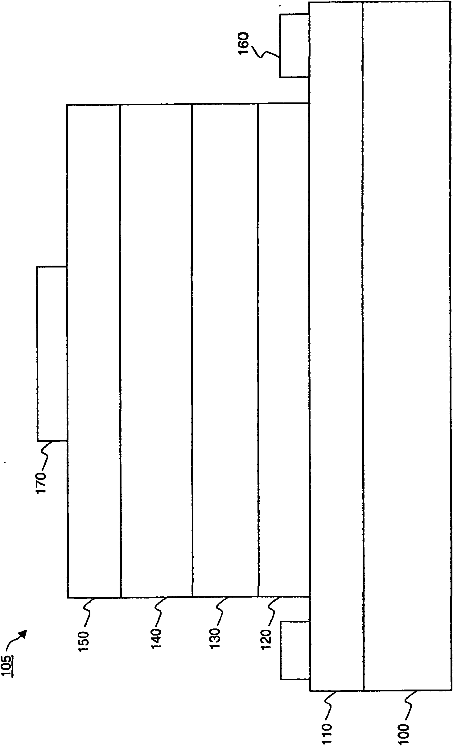
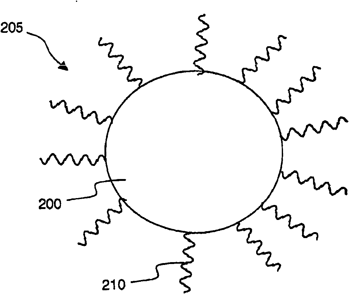
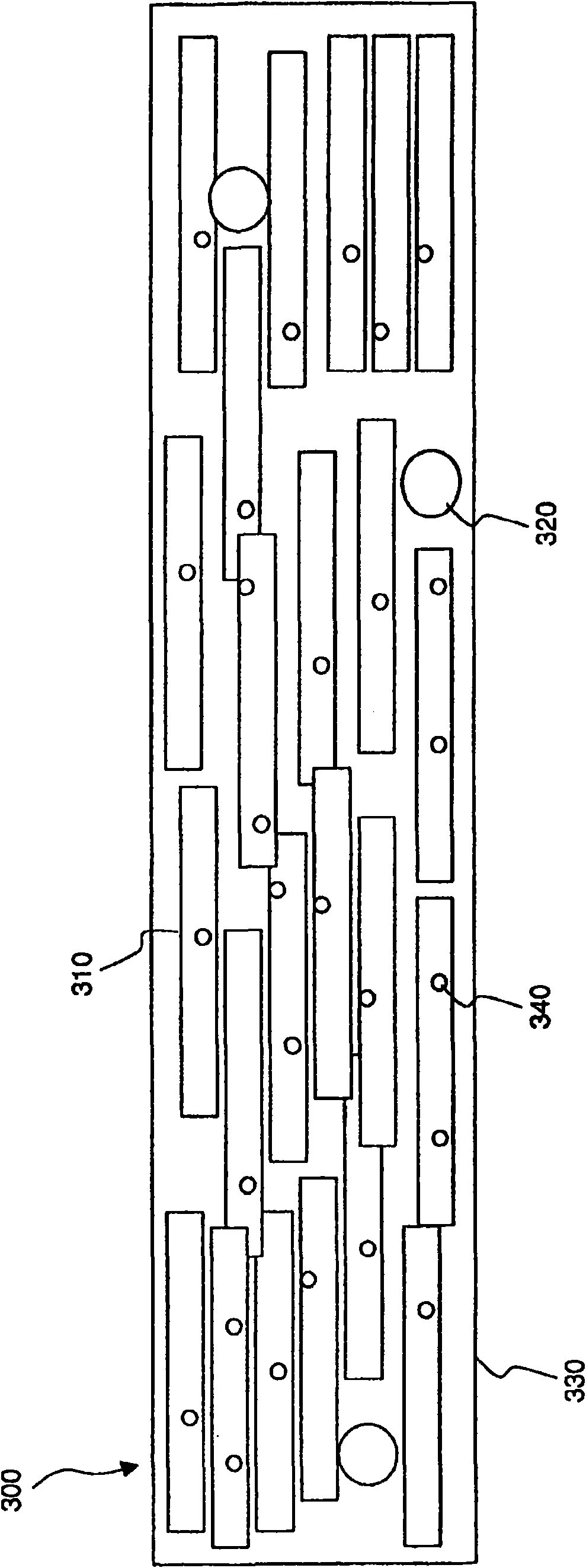
[0039] Doped and undoped semiconductor transport layers are formed on a glass substrate. The test system is ZnTe, with and without Cu doping (acceptor of ZnTe, which substitutes on cationic sites). Undoped ZnTe semiconductor nanoparticles 310 were synthesized by employing procedures commonly used to form ZnSe spherical dots (M.A. Hines et al., J. Phys. Chem. B102, 3655 (1998)). More specifically, 4 g of dried and degassed hexadecylamine (HDA) was charged into a three-necked flask, and then heated to 290° C. on a Schreck line in an argon atmosphere. For the Te precursor, a 0.25 M solution of Te in TOP (called TOPTe ). The resulting solution was clear and had a greenish-yellow appearance. In a dry box, a syringe was charged with 0.4 mmol of diethylzinc (from a 1 M solution of diethylzinc in hexane), 1.6 mmol of TOPTe and 2.0 ml of additional TOP. The contents of the syringe were quickly injected into the three-necked flask while the solution was stirred vigorously. As a res...


PUM

PropertyMeasurementUnit
particle diameteraaaaaaaaaa
thicknessaaaaaaaaaa

Abstract

A method of making an ex-situ doped semiconductor transport layer for use in an electronic device includes: growing a first set of semiconductor nanoparticles having surface organic ligands in a colloidal solution; growing a second set of dopant material nanoparticles having surface organic ligands in a colloidal solution; depositing a mixture of the first set of semiconductor nanoparticles and the second set of dopant material nanoparticles on a surface, wherein there are more semiconductor nanoparticles than dopant material nanoparticles; performing a first anneal of the deposited mixture of nanoparticles so that the organic ligands boil off the surfaces of the first and second set of nanoparticles; performing a second anneal of the deposited mixture so that the semiconductor nanoparticles fuse to form a continuous semiconductor layer and the dopant material atoms diffuse out from the dopant material nanoparticles and into the continuous semiconductor layer.

Description

Field of the invention [0001] The present invention relates to inorganic semiconductor devices comprising a charge transport layer composed of inorganic nanoparticles. Background of the invention [0002] Charge transport layers containing n-type or p-type semiconductors can be used in the fabrication of various devices such as field effect transistors, bipolar transistors, p-n diodes, light emitting diodes (LEDs), lasers, sensors, solar cells, and more. Most semiconductor devices (inorganic and organic) in use today are formed partly or completely by using expensive vacuum deposition methods. People are still looking for low-cost manufacturing methods, but so far, the device characteristics have not met the market needs. Therefore, there remains a need for low cost techniques for forming high quality inorganic charge transport layers for use in semiconductor devices. [0003] In general, both n-type and p-type materials can be referred to as charge transport materials, an...

Claims


Application Information

Patent Timeline
Patent Type & Authority Applications(China)
IPC IPC(8): H01L21/368H01L21/208
CPCH01L21/02601H01L21/02521H01L21/02628Y10S977/892
Inventor K·B·卡亨
Owner NANOCO TECH LTD
Why Eureka
Try Eureka