

Method for enhancing antistatic ability of GaN-based light-emitting diode
A light-emitting diode, gallium nitride-based technology, applied in circuits, electrical components, semiconductor devices, etc., can solve problems such as poor machining performance, device failure, and high price
- Summary
- Abstract
- Description
- Claims
- Application Information
AI Technical Summary
Problems solved by technology
Method used
Image

Examples
Embodiment 1
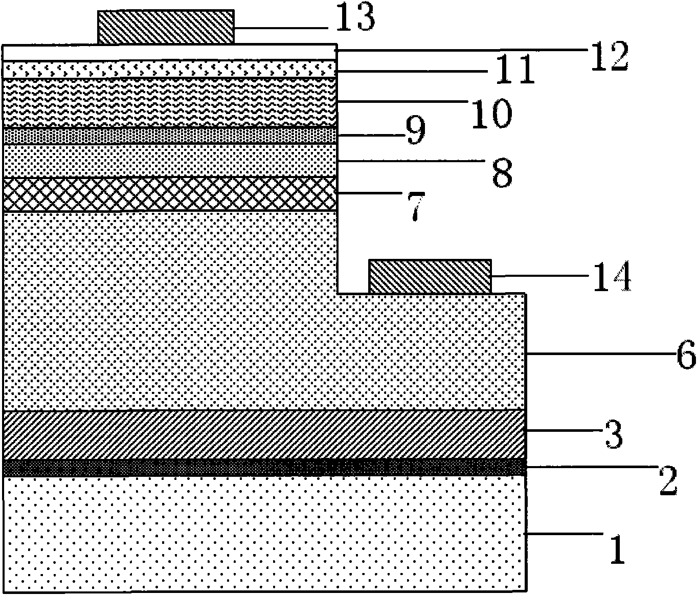
[0013] (1) Substrate 1: first anneal the sapphire substrate at a temperature of 1050°C in a pure hydrogen atmosphere, and then perform nitriding treatment;
[0014] (2) Low-temperature buffer layer 2: lower the temperature to 585°C, and grow a 20nm-thick low-temperature GaN nucleation layer;
[0015] (3) High-temperature buffer layer 3: After the growth of the low-temperature buffer layer 2 is completed, stop feeding TMGa, raise the substrate temperature by 1050° C., and perform annealing treatment on the low-temperature buffer layer 2 in situ. The annealing time is 8 minutes; after annealing , growing high-temperature undoped GaN with a thickness of 0.8 μm;
[0016] (4) After the 0.8 μm thick high-temperature undoped GaN high-temperature buffer layer 3 grows, five cycles of AlGaN / GaN (AlGaN) are grown in a pure hydrogen atmosphere. 0.2 Ga 0.8 N / GaN) superlattice structure 4, aluminum gallium nitride (Al 0.2 Ga 0.8 N) has the same thickness as gallium nitride (GaN), that i...
Embodiment 2
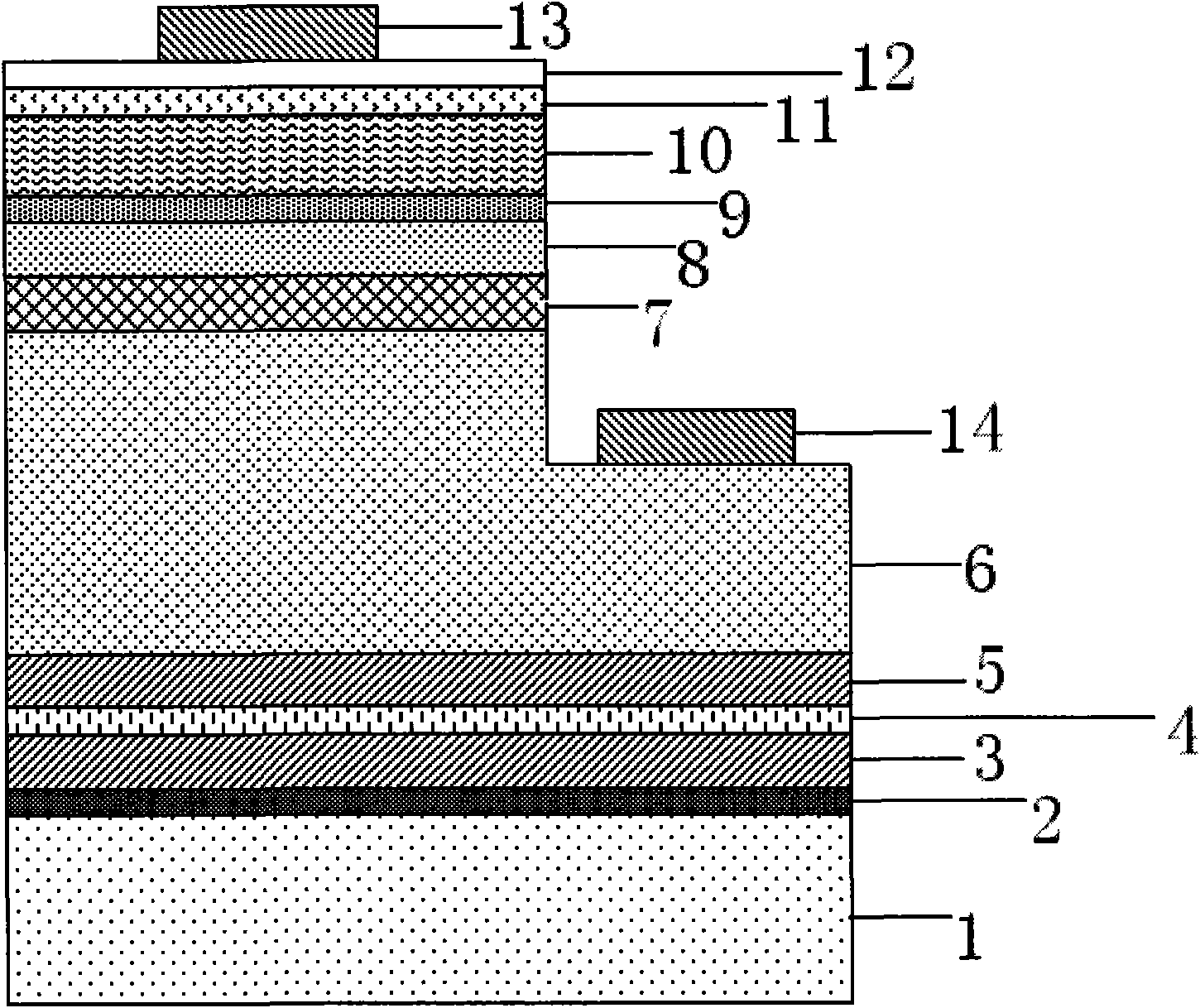
[0030] The difference between the epitaxial process of embodiment 2 and embodiment 1 is that aluminum gallium nitride / gallium nitride (Al x Ga 1-x N / GaN, 00.2 Ga 0.8 N) and the gallium nitride (GaN) well layer both have a thickness of 6nm. After the chip manufacturing process and ESD sampling test under the same conditions, it can resist static electricity: the human body model is 4000V.
Embodiment 3
[0032] The difference between the epitaxial process of embodiment 3 and embodiment 1 is that aluminum gallium nitride / gallium nitride (Al x Ga 1-x N / GaN, 0<x<1) The growth process of the superlattice structure 4 . The composition of aluminum in AlGaN is increased from 0.2 to 0.35, the growth pressure of AlGaN in the barrier layer is 30 Torr, and the growth pressure of GaN in the well layer is 100 Torr. After the chip manufacturing process and ESD sampling test under the same conditions, it can be anti-static: the human body model is 4000V. This process not only improves the anti-static performance of the chip, but also increases the optical output power by 10% compared with traditional chips.
PUM
| Property | Measurement | Unit |
|---|---|---|
| Thickness | aaaaa | aaaaa |
| Thickness | aaaaa | aaaaa |
| Thickness | aaaaa | aaaaa |
Abstract
Description
Claims
Application Information