Submount and method for manufacturing same

A manufacturing method and a mounting seat technology, which are applied in semiconductor/solid-state device manufacturing, semiconductor/solid-state device components, semiconductor devices, etc., can solve the problem of coarser surface roughness of electrode layers, larger surface roughness of substrates, and rising costs, etc. question

Inactive Publication Date: 2010-02-24
DOWA ELECTRONICS MATERIALS CO LTD
View PDF5 Cites 5 Cited by
  • Summary
  • Abstract
  • Description
  • Claims
  • Application Information

AI Technical Summary

Problems solved by technology

In the case of using an adhesive layer of noble metal, there is a big problem of cost increase
[0032] In the case of forming electrodes on the submount by the lift-off method, the roughness of the substrate surface tends to increase, which has the effect of improving the bonding strength of the electrode layer itself formed on the substrate surface. The problem that the surface roughness of the electrode layer formed on the surface of the substrate in the rough state also becomes rough

Method used


Image

  • Submount and method for manufacturing same
  • Submount and method for manufacturing same
  • Submount and method for manufacturing same

Examples


Embodiment 1

[0157] Hereinafter, the present invention will be described in more detail based on examples.

[0158] First, a method of manufacturing the submount will be described.

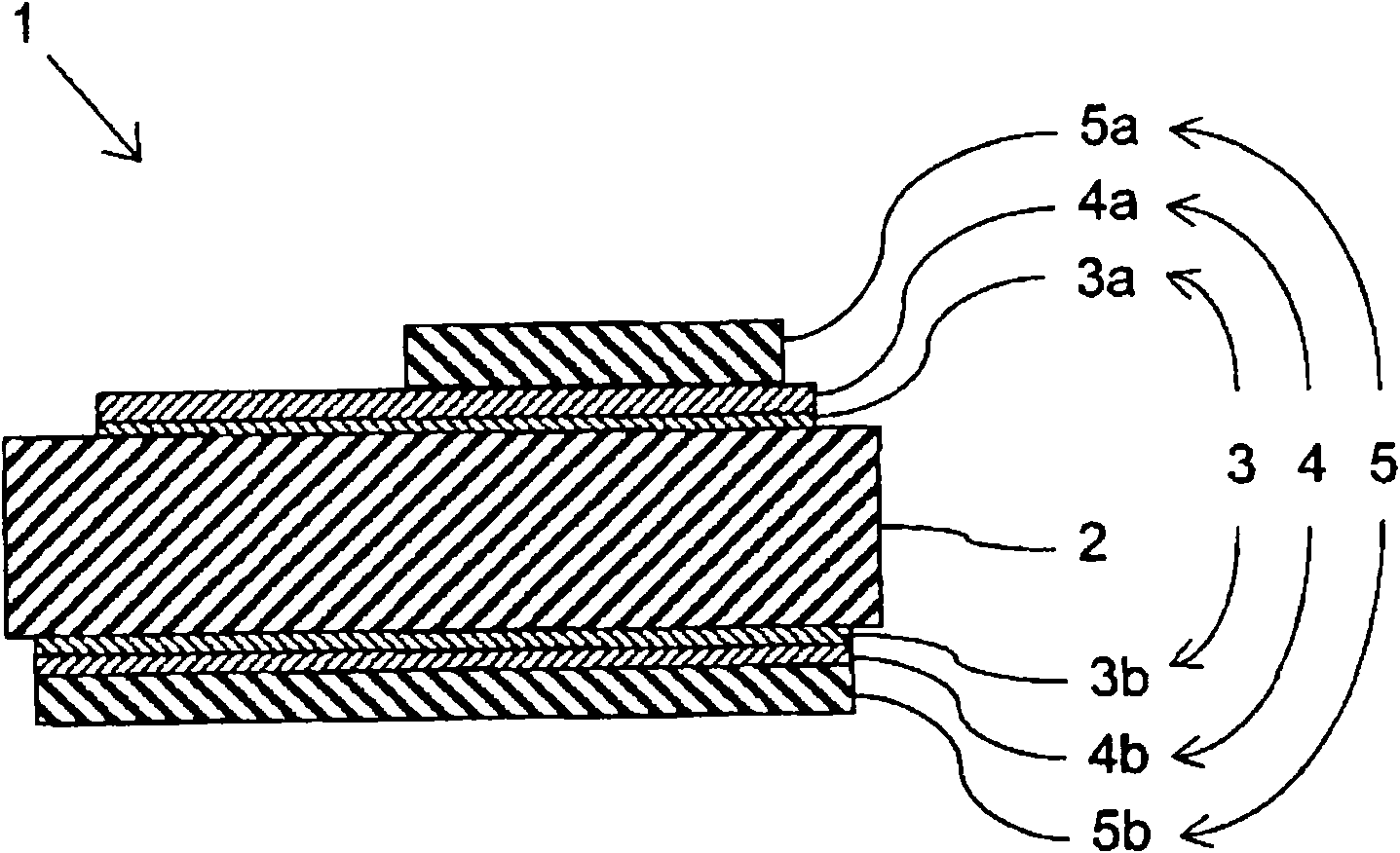
[0159] Both sides of a 55 mm square sintered aluminum nitride substrate 2 with a high thermal conductivity (230 W / mK) and a thickness of 0.3 mm are ground by a grinding device, and finishing grinding is performed by a polishing device to make the average roughness of the aluminum nitride substrate 2 The degree (Ra) is 0.07 μm.

[0160] The polished aluminum nitride substrate 2 was cleaned to clean the surface, and a 0.05 μm substrate protection layer 3 a made of titanium was deposited on the entire surface of the substrate 2 by a vacuum evaporation device.

[0161] Next, for patterning by photolithography, the entire surface of the substrate on which the substrate protection layer 3a is deposited is uniformly coated with a resist using a spin coater, and then baked in a baking oven for a predetermined period ...

Embodiment 2

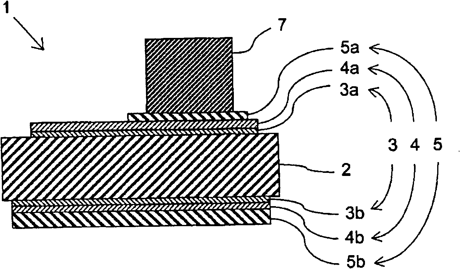
[0166] The submount 1 of Example 2 was manufactured in the same manner as in Example 1 except that the average roughness (Ra) of the aluminum nitride substrate 2 was 0.04 μm.

[0167] Next, comparative examples will be described.

Embodiment 3

[0196] Hereinafter, the present invention will be described in more detail based on Examples 3 and 4. First, the method of manufacturing the submount of the third embodiment will be described.

[0197] Both sides of a high thermal conductivity (230 W / mK) aluminum nitride sintered substrate (55 mm square, 0.3 mm thick) were ground by a grinding device. In addition, finish grinding is performed using a polishing device. The polished aluminum nitride sintered substrate 12 is cleaned to clean the surface, and a resist is uniformly applied to the entire surface of the submount substrate 12 by a spin coater for patterning by photolithography. Predetermined baking is performed in a baking oven, and gamma-ray contact exposure is performed using a mask aligner. The mask for exposure is designed so that 2500 pieces can be simultaneously patterned with a submount size of 1mm square. After the exposure, the resist on the portion of the electrode layer is dissolved with a developer to e...


PUM

PropertyMeasurementUnit
surface roughnessaaaaaaaaaa
mean roughnessaaaaaaaaaa

Abstract

A submount with an electrode layer having excellent wettability in soldering and method of manufacturing the same are disclosed. A submount (1) for having a semiconductor device mounted thereon comprises a submount substrate (2), a substrate protective layer (3) formed on a surface of the submount substrate (2), an electrode layer (4) formed on the substrate protective layer (3) and a solder layer(5) formed on the electrode layer (3) wherein the electrode layer (4) is made having an average surface roughness of less than 1 [mu]m. The reduced average surface roughness of the electrode layer (4) improves wettability of the solder layer (5), allowing the solder layer (5) and a semiconductor device to be firmly bonded together without any flux therebetween. A submount (1) is thus obtained which with the semiconductor device mounted thereon is reduced in heat resistance, reducing its temperature rise and improving its performance and service life.

Description

[0001] This application is a divisional application with an application date of March 17, 2006, a Chinese patent application number of 200680012991.9, and an invention title of "Auxiliary Mounting Seat and Its Manufacturing Method". technical field [0002] The present invention relates to a submount used in a semiconductor device and a method of manufacturing the same. Background technique [0003] Usually, when a semiconductor device is packaged, it is mounted on a heat sink or a heat sink to dissipate heat generated from the semiconductor device. In order to improve heat dissipation characteristics, a substrate with high thermal conductivity, that is, a submount member may be interposed between the semiconductor device and the heat dissipation plate. Aluminum nitride (AlN) or the like is known as a substrate having such a high thermal conductivity. [0004] When bonding the submount to the semiconductor device, the bonding strength is required as one of the requirements....

Claims


Application Information

Patent Timeline
Patent Type & Authority Applications(China)
IPC IPC(8): H01L23/14H01L21/48H01L33/00
CPCH01L2924/0103H01L2924/01029H01L2924/01074H01L2924/0105H01L2924/01078H01L2924/01042H01L2924/01028H01L2924/01079H01L2924/01049H01L2924/014H01L2924/01013H01L2224/32225H01L2924/1301
Inventor 大鹿嘉和中野雅之
Owner DOWA ELECTRONICS MATERIALS CO LTD
Why Eureka
Try Eureka