Multilayer interconnection packaging structure of silica-based embedded microwave multi chip module and manufacturing method

A multi-layer interconnection and packaging structure technology, which is applied in semiconductor/solid-state device manufacturing, electrical components, electric solid-state devices, etc., can solve the problems of large loss and achieve the effects of reducing loss, reducing cost, and high thermal conductivity

Inactive Publication Date: 2010-02-24
SHANGHAI INST OF MICROSYSTEM & INFORMATION TECH CHINESE ACAD OF SCI
View PDF0 Cites 30 Cited by
  • Summary
  • Abstract
  • Description
  • Claims
  • Application Information

AI Technical Summary

Problems solved by technology

Then, a ground shielding layer is prepared on the silicon substrate with an embedded cavity. This method effectively isolates

Method used


Image

  • Multilayer interconnection packaging structure of silica-based embedded microwave multi chip module and manufacturing method
  • Multilayer interconnection packaging structure of silica-based embedded microwave multi chip module and manufacturing method
  • Multilayer interconnection packaging structure of silica-based embedded microwave multi chip module and manufacturing method

Examples


Embodiment Construction

[0032] Embodiments of the present invention will be further specifically described below with reference to the accompanying drawings in order to fully demonstrate the advantages and positive effects of the present invention. The scope of the present invention is not limited to the following examples.

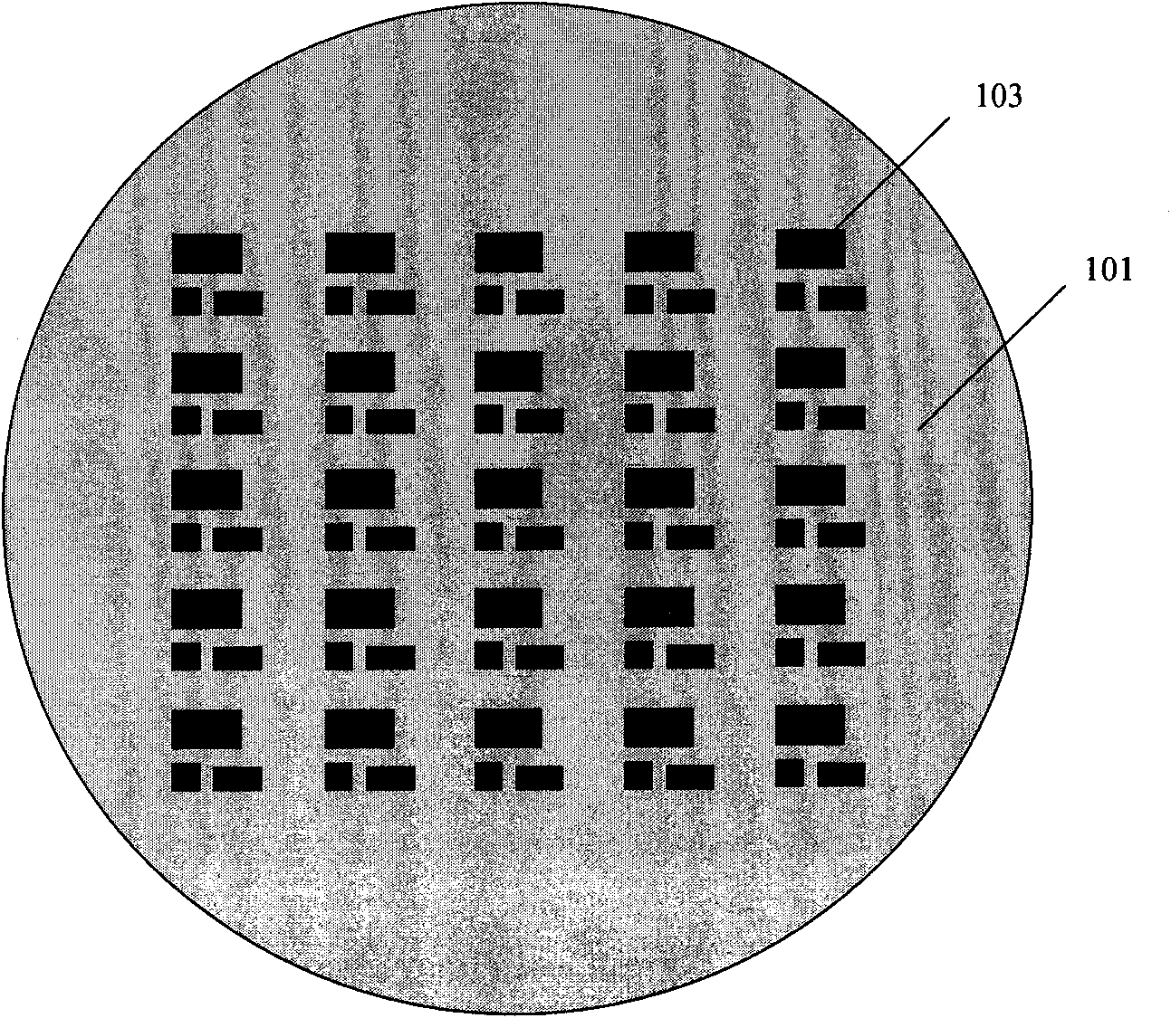
[0033] exist figure 1 In the silicon substrate 101, a 5×5 cell array is distributed on the front side of the silicon substrate 101, and each cell has three cavities 103 of different sizes, which are suitable for embedding chips of different sizes. The cavities 103 are formed by wet etching. The distribution of the unit array is not limited to 5×5, 5×5 is just an example, and the number of cavities in each unit is not limited to 3, and the size is different, depending on the embedded microwave chip.

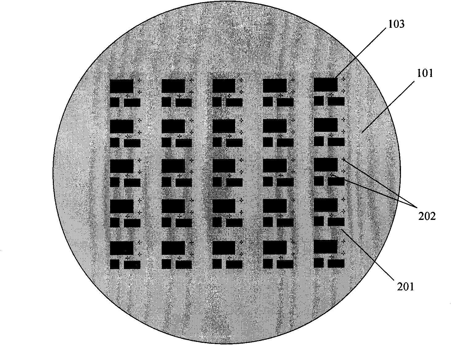
[0034] exist figure 2 In the present invention, the ground shielding layer 201 is prepared on the silicon substrate containing the embedded cavity, and the ground shielding layer...


PUM

PropertyMeasurementUnit
Thicknessaaaaaaaaaa
Thicknessaaaaaaaaaa

Abstract

The invention provides a multilayer interconnection packaging structure of an embedded microwave multi chip with a silicon chip as a substrate and a manufacturing method. The invention is characterized by utilizing the low-cost silicone chip as the chip embedded substrate and using wire bonding and ball mounting technology to prepare gold bumps, realizing short-distance interconnection between microwave chips, using a low-k liquid or colloidal polymer as a dielectric layer, realizing the multilayer interconnection structure of a metal/organic polymer by combining wafer level processing technics such as photoetching, electroplating, chemical mechanical polishing and the like and realizing system integration of active and passive devices. The whole packaging structure has higher packaging integration and lower high-frequency transmission loss. The structure can effectively integrate varied function device units, reduce the interconnection loss among the devices and improve the propertiesof the whole module while improving the density and integration of packaging and reducing the cost of packaging.

Description

technical field [0001] The invention relates to a microwave multi-chip module (Microwave Multi Chip Module, abbreviated as MMCM) silicon-based embedded packaging structure realized by multilayer interconnection technology, which belongs to the field of microwave device packaging. Background technique [0002] Multi-chip module (Multi Chip Module, abbreviated as MCM), refers to the integration of multiple bare or / and packaged integrated circuit chips and single or multiple passive components, such as resistors, capacitors, inductors, etc., into a multilayer A technology that forms a system or functional module on a high-density substrate. [0003] MCM adopts the method of directly mounting and connecting the bare chip to the substrate. The interconnection distance between the chips is short, which reduces the inductance and impedance of the interconnection line, thus reducing the transmission delay time of the signal while increasing the assembly density. , to increase the t...

Claims


Application Information

Patent Timeline
IPC IPC(8): H01L23/522H01L23/48H01L23/13H01L21/50H01L21/60
CPCH01L2924/01074H01L2924/01087H01L2924/10329H01L2924/01005H01L2924/10253H01L2924/01082H01L24/82H01L2924/01019H01L2924/01006H01L2924/01067H01L2924/01079H01L2924/14
Inventor 耿菲丁晓云罗乐
Owner SHANGHAI INST OF MICROSYSTEM & INFORMATION TECH CHINESE ACAD OF SCI
Why Eureka
Try Eureka