A method of making a smooth surface microstructure

A manufacturing method and technology of curved surface structure, applied in the field of MEMS, can solve the problems of limited application range, positive photoresist materials are easily eroded by acid and alkali or organic reagents, and limit the height of microstructures, which achieves a simple process and is conducive to expansion. applied effect

Active Publication Date: 2011-12-28
SHANGHAI INST OF MICROSYSTEM & INFORMATION TECH CHINESE ACAD OF SCI
View PDF0 Cites 0 Cited by
  • Summary
  • Abstract
  • Description
  • Claims
  • Application Information

AI Technical Summary

Problems solved by technology

However, the above two technologies have great limitations in practical application. Gray-scale photomask technology requires expensive, high-resolution gray-scale photomasks, which are complex to process and costly; and photolithography Positive photoresist is usually used in glue reflow technology, and its spin coating thickness is often small (single spin coating thickness <50 μm), which limits the height of the microstructure that can be obtained, and the positive photoresist material itself is often easy to Affected by acid, alkali or organic reagents, the application range is limited

Method used


Image

  • A method of making a smooth surface microstructure
  • A method of making a smooth surface microstructure
  • A method of making a smooth surface microstructure

Examples


Embodiment 1

[0016] The substantive features and remarkable progress of the present invention will be further described below in conjunction with the accompanying drawings using SU-8 photoresist.

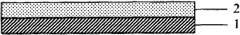
[0017] 1. Take the cleaned silicon wafer and bake it at 150°C for 20 minutes. After cooling to room temperature, spin-coat the first layer of SU-8 photoresist and place it on a hot plate for 1 minute at 65°C. Bake for 15 minutes, then cool to room temperature, as figure 1 shown.

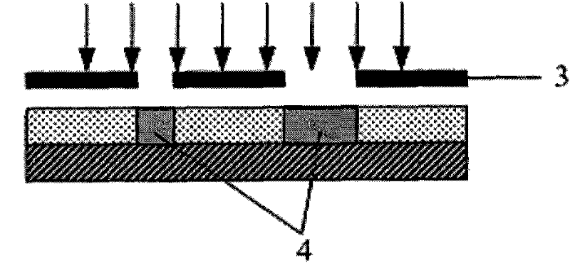
[0018] 2. Expose the coated and soft-baked substrate through a photomask. At this time, the PAG in the exposed area of ​​​​the first layer of SU-8 photoresist will be decomposed to generate photoacid, such as figure 2 shown.

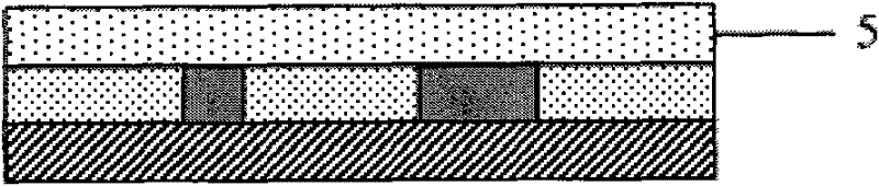
[0019] 3. Spin-coat the second layer of SU-8 photoresist directly on the surface of the first layer of SU-8 photoresist after exposure within 1 hour, such as image 3 shown.

[0020] 4. Place the silicon substrate spin-coated with the second layer of photoresist on a hot plate and bake at 95...

Embodiment 2

[0023] Utilize the process method of making the SU-8 curved surface microstructure that embodiment 1 proposes to make microlens arrays with different curvatures (such as Figure 6 As shown), the curvature of the microlens can be controlled by adjusting the thickness of the bottom layer (first layer) SU-8 photoresist and the size and shape design of the light-transmitting structure of the photolithography mask. The thickness of the bottom layer SU-8 photoresist is between Between 10 μm-1000 μm, the shape of the light-transmitting structure of the photolithographic mask can be a regular polygon or a circle, and the side length of the regular polygon or the diameter of the circle is 10 μm-1000 μm. The fabricated microlens array can be applied to fields such as flat panel display, three-dimensional stereoscopic imaging, fiber optic coupler, micro-focusing, and micro-projection.


PUM

PropertyMeasurementUnit
thicknessaaaaaaaaaa
diameteraaaaaaaaaa

Abstract

The invention discloses a method for making a smooth curved surface microstructure, which is characterized in that the method uses negative chemically amplified photoresist (chemically amplified photoresist) as the material for making the smooth curved surface microstructure, and first spin-coats the first microstructure on a substrate. One layer of negative chemically amplified photoresist, soft-baked and exposed, and then directly spin-coated a second layer of negative chemically amplified photoresist on the first layer of negative chemically amplified photoresist, and post-baked; after use During the baking process, the photoacid generated after the exposure of the first layer of photoresist diffuses isotropically, catalyzes the cross-linking of photoresist molecules in the exposed area and its adjacent diffusion area, and develops a microstructure with smooth curved surface characteristics. Compared with the traditional gray-scale mask technology and photoresist reflow method, the manufacturing method of the smooth surface microstructure proposed by the present invention has the characteristics of simple processing, low cost, stable structure and the like.

Description

technical field [0001] The invention relates to a manufacturing method of a smooth curved surface microstructure, and the manufacturing method provided can be applied to the field of MEMS (Micro Electromechanical System, ie micro-electromechanical system). Background technique [0002] In recent years, MEMS technology has received widespread attention and rapid development. Through miniaturization and integration, MEMS devices and systems such as micro-sensors, micro-actuators, and micro-structures have been produced that meet the requirements of various fields. These devices and systems combine automation and intelligence. It will have a major impact on the development of industry and agriculture, information, environment, bioengineering, medical treatment, space technology, national defense and science. At present, MEMS devices are generally manufactured by traditional microelectronic processing technology, and often have neat and clear corners. Their 3D surfaces are usual...

Claims


Application Information

Patent Timeline
Patent Type & Authority Patents(China)
IPC IPC(8): B81C1/00B81B7/02G03F7/00G03F7/038G03F1/14
Inventor 李刚陈强孙晓娜赵建龙
Owner SHANGHAI INST OF MICROSYSTEM & INFORMATION TECH CHINESE ACAD OF SCI
Why Eureka
Try Eureka