
Large size conductive substrate thick circuit write-through device and write-through technology thereof

A conductive substrate and large-format technology, which is applied in the field of repeated direct writing devices and high-precision positioning, can solve the problems of high exposure and etching costs, slow processing speed, and low line yield, and achieve high performance in positioning and repeated direct writing , low wiring cost and large processing area

Inactive Publication Date: 2010-03-03
杨飞
View PDF0 Cites 3 Cited by
  • Summary
  • Abstract
  • Description
  • Claims
  • Application Information

AI Technical Summary

Problems solved by technology

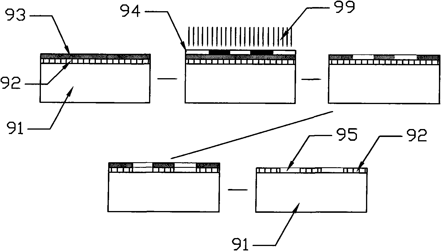
[0007] However, these existing direct writing processes have more or less defects, such as high cost of plate making and ink in the wiring process of screen printing, and poor positioning and repeated direct writing accuracy, and the yield rate of lines less than 100 μm Very low; the wiring process of mask lithography is expensive for mask making, exposure and etching, and direct writing is not cost-effective for large-format situations; the processing format of platform-moving laser direct writing is determined by the stroke of the X and Y servo motors , and the processing speed is particularly slow when it is a non-X or Y-direction line such as an arc or a broken line; while the processing speed of the single-galvanometer + platform stepping laser direct writing process is slow; the single-format precision is high, but when combined with the step The precision of the advanced large-format direct writing process is poor

Method used


Image

  • Large size conductive substrate thick circuit write-through device and write-through technology thereof
  • Large size conductive substrate thick circuit write-through device and write-through technology thereof
  • Large size conductive substrate thick circuit write-through device and write-through technology thereof

Examples


Embodiment Construction

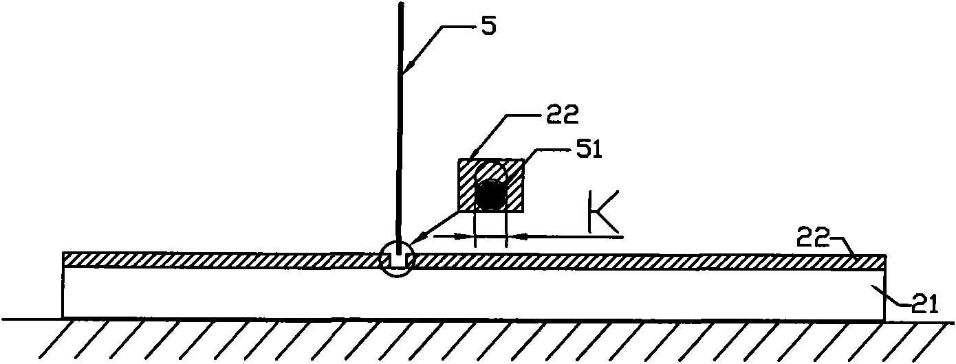
[0026] Such as image 3 As shown, it is a schematic diagram of the principle of the laser direct writing technology based on the thick line direct writing process for large-format conductive substrates in the present invention. The conductive substrate generally consists of a non-conductive substrate 21 and a thin conductive film layer 22. The conductive film layer can be either a conductive plating layer or a conductive coating layer, and can be either a single-layer structure or a multi-layer stack. According to the thickness and energy absorption characteristics of the conductive film layer on the conductive substrate, laser light 5 with specific power and frequency can be selected to irradiate the conductive substrate. The diameter and energy density of the laser spot 51 thus control the etching width K. When the spot focus 51 of the laser 5 moves in a certain direction at a certain speed, a continuous etching line can be drawn on the conductive substrate. Cooperating wi...


PUM


Abstract

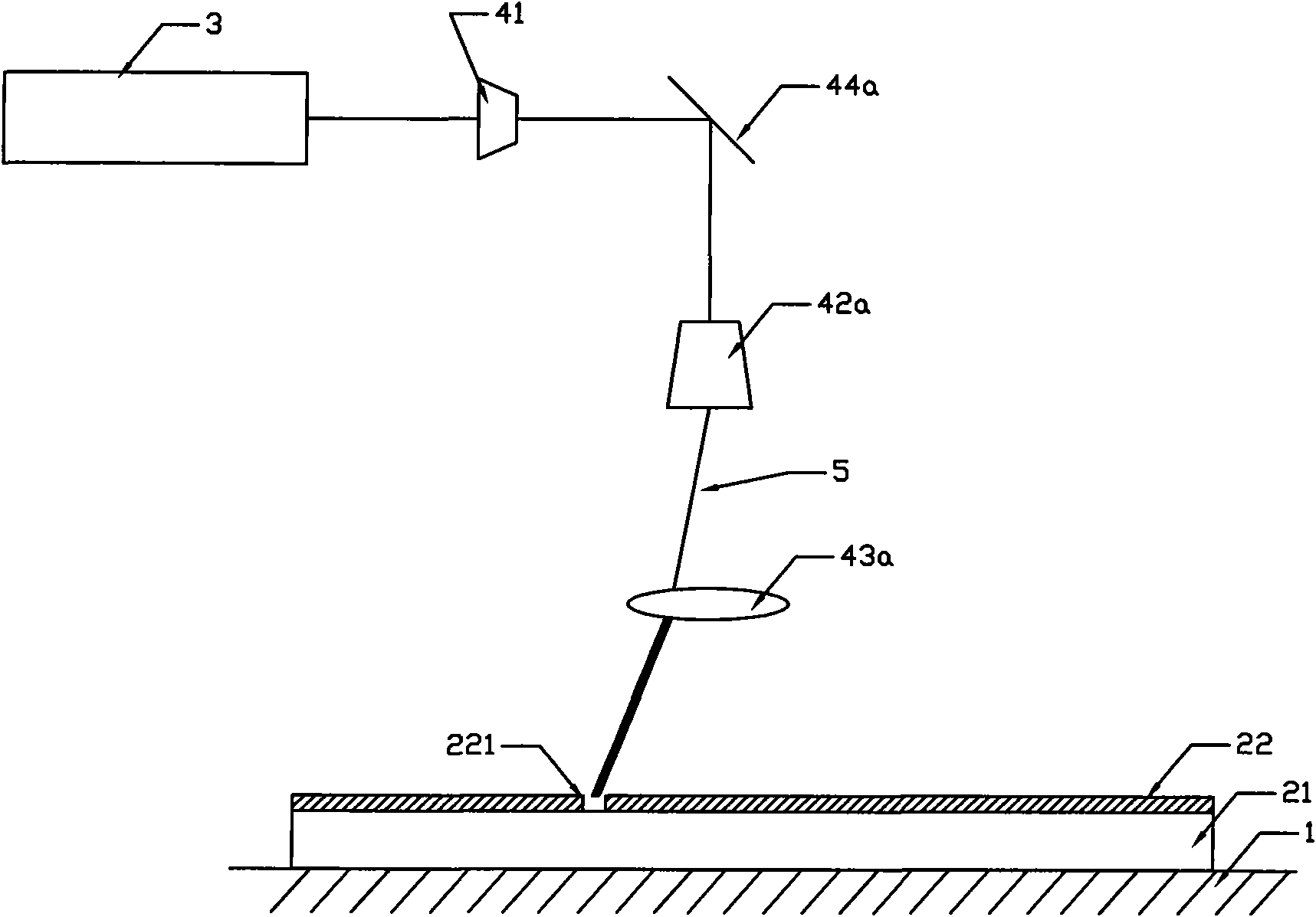
The invention discloses a large size conductive substrate thick circuit write-through device and write-through technology thereof. The device comprises a controller, a platform, a conductive substrateto be written through, a laser transmitter and a polarizer unit arranged on the laser path; wherein the platform is static, and more than one polarizer unit are arranged, so as to form a multi-polarizer array above the platform. The controller drives the multi-polarizer array to control the focus of the laser path to move at certain speed along etching direction, the multi-polarizer array with relatively fixed mechanical structure is utilized to realize circuit detail drawing write-through on the full size of a conductive substrate, thus providing a feasible technology approach for rapidly and accurately write-through preparation of thick circuit with wire width more than 30 microns on a large size conductive substrate. The invention has the special effects of low wiring cost, minimum wire width and minimum wire distance as short as 30 microns, large processing size, fast processing speed and high location and repeated write-through performance.

Description

technical field [0001] The invention relates to a direct writing device and process for preparing micro-thick and thin conductive lines on a conductive substrate, in particular to a device and a process capable of rapid processing, high-precision positioning, and repeated direct writing on a large-format conductive substrate. Background technique [0002] At present, laser direct writing systems with different structures are used in many industries such as integrated circuit manufacturing, micro-optical component processing, MEMS, optical detection, and optical anti-counterfeiting. Therefore, the development of laser direct writing system has attracted much attention. The existing relatively mature wiring technology includes: screen printing, single-galvanometer platform stepping laser direct writing, platform moving laser direct writing and mask lithography, etc. Specifically: [0003] Screen printing: After the screen screen is covered with photosensitive glue, it is expo...

Claims


Application Information

Patent Timeline
Patent Type & Authority Applications(China)
IPC IPC(8): G03F7/20G02B26/08
Inventor 文谏黄良杰李春宝高委严翠萍
Owner 杨飞
Learn More