Coarsening solution for electroplating pretreatment on surface of semiconductor N\P type cooling wafer and related electroplating pretreatment process

A technology of pre-plating treatment and cooling wafers, which is applied to semiconductor devices, post-processing, post-processing details, etc., can solve the problems of low product qualification rate, low production efficiency, high production cost, etc., to reduce operating personnel and improve production efficiency , the effect of easy preparation

Active Publication Date: 2010-05-05
江苏富乐华半导体科技股份有限公司
View PDF0 Cites 9 Cited by
  • Summary
  • Abstract
  • Description
  • Claims
  • Application Information

AI Technical Summary

Problems solved by technology

[0002] For the treatment before electroplating on semiconductor N\P type refrigeration materials, the general treatment method is physical treatment, that is, the method of sand blasting and nickel spraying on the surface of semiconductor materials is used to increase the roughness of the material surface and deposit a conductive nickel layer. To improve the bonding force of the coating, but because of the impact of high temperature and high pressure during sandblasting and nickel spraying, it is easy to cause cracking of the wafer, which makes the production cost high, and the product qualification rate is low, and the production efficiency is low

Method used


Image

  • Coarsening solution for electroplating pretreatment on surface of semiconductor N\P type cooling wafer and related electroplating pretreatment process
  • Coarsening solution for electroplating pretreatment on surface of semiconductor N\P type cooling wafer and related electroplating pretreatment process
  • Coarsening solution for electroplating pretreatment on surface of semiconductor N\P type cooling wafer and related electroplating pretreatment process

Examples


Embodiment 1

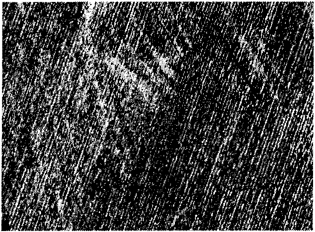
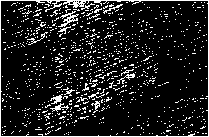
[0028] P-type wafers with a diameter of ¢2 cm and a thickness of 0.15 cm are degreased to remove surface cutting fluid and pollutants, and the surface is relatively flat after washing (such as figure 1 shown), immersed in a solution composed of 5% hydrofluoric acid (V / V), 20% nitric acid (V / V), 0.5 (g / l) sodium dodecylbenzenesulfonate, and the remainder of water , etch at a temperature of 25-30°C for 2-10 minutes, take it out and wash it with water, and obtain a roughened layer with a roughness of 14-25um (such as figure 2 shown), activation, impact nickel plating for 2 to 5 minutes after water washing, and then transfer to the desired coating.

Embodiment 2

[0030] P-type wafers with a diameter of ¢2 cm and a thickness of 0.15 cm, after degreasing to remove surface cutting fluid and pollutants, and washing with water, the surface is relatively smooth, and the main components of immersion are hydrofluoric acid (V / V) 20%, nitric acid (V / V ) 40%, sodium dodecylbenzenesulfonate 5 (g / l), and the rest of water to form a solution, etch at a temperature of 25-30°C for 2-10 minutes, take it out and wash it, and obtain a roughness between 14-25um. After roughening, activation, and water washing, impact nickel plating for 2 to 5 minutes, and then transfer to the desired coating.

Embodiment 3

[0032] P-type wafers with a diameter of ¢2 cm and a thickness of 0.15 cm are degreased to remove surface cutting fluid and pollutants, and the surface is relatively smooth after washing with water. The main components of immersion are hydrofluoric acid (V / V) 10%, nitric acid (V / V ) 30%, sodium dodecylbenzene sulfonate 3 (g / l) water balance solution, etch at a temperature of 25-30°C for 2-10 minutes, take it out and wash it, and obtain a roughness between 14-25um After roughening, activation, and water washing, impact nickel plating for 2 to 5 minutes, and then transfer to the desired coating.


PUM


Abstract

The invention relates to a coarsening solution for electroplating pretreatment on a surface of a semiconductor N\P type cooling wafer, which comprises a solution A and a solution B preferably, wherein the solution A comprises 5-20% (volume) of hydrofluoric acid, 20-40% (volume) of nitric acid, 0.5-5g/L sodium dodecyl sulfate and the balance of water; and the solution B comprises 10-50g/L potassium bromate, 2-10% (volume) of nitric acid and the balance of water. The invention also provides a process for electroplating pretreatment on the surface of the semiconductor N\P type cooling wafer by using the coarsening solution, which comprises the following steps: soaking the degreased semiconductor N\P type cooling wafer in the solution A for etching and coarsening, and then, soaking the wafer in the solution B for ash removing treatment. The electroplating pretreatment process of the invention can increase the bonding force between a substrate and a nickel layer, can improve the cooling temperature difference and performance of the cooling wafer, can not cause the fracture of the wafer, reduces the production cost, and improves the qualified rate and the production efficiency of products.

Description

technical field [0001] The invention relates to the technical field of surface electroplating treatment, in particular to the technical field of surface electroplating treatment of semiconductor refrigeration materials (antimony, bismuth, selenium, tellurium mixed crystals), specifically refers to a semiconductor N\P type refrigeration chip surface electroplating pre-plating The treated roughening solution and related electroplating pretreatment process. Background technique [0002] For the treatment before electroplating on semiconductor N\P type refrigeration materials, the general treatment method is physical treatment, that is, the method of sand blasting and nickel spraying on the surface of semiconductor materials is used to increase the roughness of the material surface and deposit a conductive nickel layer. To improve the bonding force of the coating, but because of the impact of high temperature and high pressure during sandblasting and nickel spraying, it is easy ...

Claims


Application Information

Patent Timeline
Patent Type & Authority Applications(China)
IPC IPC(8): C25D7/12C25D5/54C30B33/10
Inventor 陈良杰
Owner 江苏富乐华半导体科技股份有限公司
Why Eureka
Try Eureka