Surface roughening method of p-GaN layer or ITO layer in GaN-based LED chip structure

A LED chip and surface roughening technology, applied to electrical components, circuits, semiconductor devices, etc., can solve problems such as difficult process control, high technical requirements, and increased forward bias voltage, and achieve easy process control, simple manufacturing process, The effect of increasing the probability of device surface

Inactive Publication Date: 2010-05-05
SOUTH CHINA NORMAL UNIVERSITY
View PDF0 Cites 55 Cited by
  • Summary
  • Abstract
  • Description
  • Claims
  • Application Information

AI Technical Summary

Problems solved by technology

[0004] In the surface roughening methods that have been proposed so far, although the brightness of LEDs has been improved to varying degrees

Method used


Image

  • Surface roughening method of p-GaN layer or ITO layer in GaN-based LED chip structure
  • Surface roughening method of p-GaN layer or ITO layer in GaN-based LED chip structure
  • Surface roughening method of p-GaN layer or ITO layer in GaN-based LED chip structure

Examples


Embodiment 1

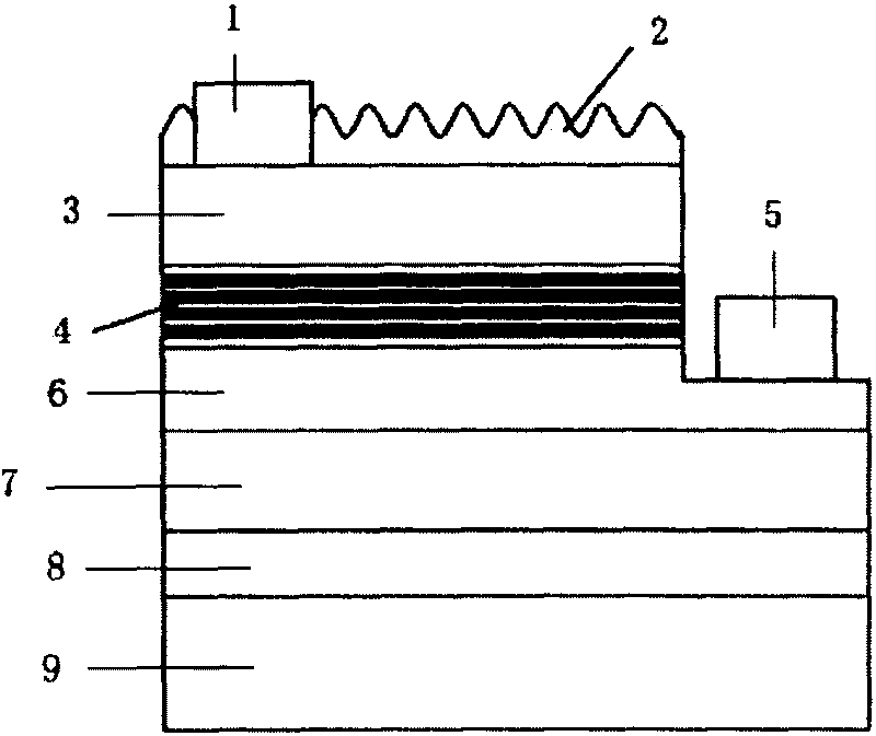
[0032] The method for improving the light output rate of LED by roughening the surface of the ITO current spreading layer mainly includes the following steps:

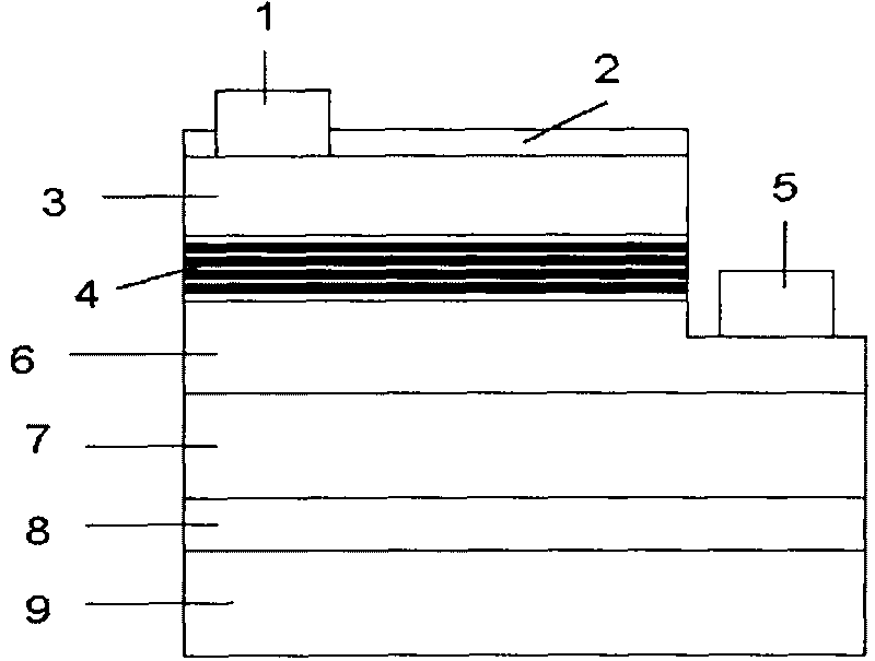
[0033](1) Low-temperature GaN buffer layer, undoped GaN layer, n-GaN layer, multiple quantum well layer, p-GaN layer and evaporated ITO are sequentially grown on the semiconductor substrate by metal organic chemical vapor deposition (MOCVD) layered structure. Wherein the material of the semiconductor substrate is sapphire;

[0034] (2) Perform MESA photolithography and ICP etching on the grown epitaxial wafer until the n-type GaN is exposed;

[0035] (3) Electron beam deposition is used to deposit a layer of ITO thin film on the substrate after MESA lithography as the current spreading layer, and the thickness of the thin film is 350nm;

[0036] (4) Weigh 3g of nano-nickel particles into 30mL of ethanol, add 0.6g of citric acid, and ultrasonically disperse for 15min. If the surface of nickel nanoparticles is oxidize...

Embodiment 2

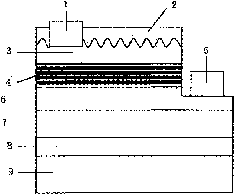
[0042] The method for improving the light output rate of GaN-based LEDs by roughening the surface of the p-GaN layer mainly includes the following steps:

[0043] (1) The low-temperature GaN buffer layer, undoped GaN layer, n-GaN layer, multi-quantum well layer, p-GaN layer and evaporated ITO are sequentially grown on the semiconductor substrate by metal-organic chemical vapor deposition (MOCVD) layered structure. Among them, the p-GaN layer is composed of a 10nm thick p-GaN layer and a 180nm thick magnesium-doped p-type GaN layer, and the material of the semiconductor substrate is silicon;

[0044] (2) Weigh 3g of nano-nickel particles in 30mL of ethanol, add 0.6g of oleic acid, and disperse ultrasonically for 10min. Before the dispersion is prepared, the surface of nickel nanoparticles is deoxidized, that is, the surface oxide of nano-nickel powder is removed. The specific operation is to put dilute hydrochloric acid (1:10) and nano-nickel powder into a beaker with a mass r...


PUM

PropertyMeasurementUnit
Diameteraaaaaaaaaa
Thicknessaaaaaaaaaa
Thicknessaaaaaaaaaa

Abstract

The invention discloses a surface roughening method of a p-GaN layer or an ITO layer in a GaN-based LED chip structure. The method comprises the following steps: (1) growing a low-temperature GaN buffer layer, an undoped GaN layer, an n-GaN layer, a multiple quantum well layer, a stack-up structure of the p-GaN layer and an extended layer evaporating ITO current on a semiconductor substrate in sequence; and (2) preparing monolayer nickel nano particles as a mask, and preparing a roughening structure on the p-GaN layer or the ITO layer. The method of the invention has simple steps, low cost, good roughening effect; by carrying out surface roughening on the p-GaN layer or the ITO layer of the GaN-based LED by the method of the invention, the total reflection of the photon in the chip can be inhibited and the light outgoing efficiency of the devices can be improved.

Description

technical field [0001] The invention relates to the field of optoelectronic devices, in particular to a method for roughening the surface of a p-GaN layer or an ITO layer in a GaN-based LED chip structure. Background technique [0002] In recent years, light-emitting diodes (LEDs) have undoubtedly become one of the most valued light source technologies. On the one hand, the LED has the characteristics of small size; on the other hand, the LED has the power-saving characteristics of low current and low voltage driving. Theoretically, it is estimated that the luminous efficiency of semiconductor LED lighting can reach or even exceed 10 times that of incandescent lamps and 2 times that of fluorescent lamps. At the same time, it also has many advantages such as firm structure, strong impact resistance and earthquake resistance; super long life, up to 100,000 hours; no infrared and ultraviolet radiation; no mercury, which is conducive to environmental protection and many other a...

Claims


Application Information

Patent Timeline
IPC IPC(8): H01L33/00H01L33/06H01L33/02H01L33/14H01L33/22H01L33/44
Inventor 何安和章勇何苗范广涵
Owner SOUTH CHINA NORMAL UNIVERSITY
Why Eureka
Try Eureka