Optical receiving assembly for hundred trillion-grade 850nm optical communication and preparation method thereof

A technology for optical receiving components and optical communication, which is applied in the coupling of optical waveguides, semiconductor/solid-state device manufacturing, electrical components, etc. performance, reduced packaging costs, and the effect of reducing system components

Inactive Publication Date: 2010-06-02
XIAMEN UNIV
View PDF0 Cites 5 Cited by
  • Summary
  • Abstract
  • Description
  • Claims
  • Application Information

AI Technical Summary

Problems solved by technology

[0004] The purpose of the present invention is to provide a kind of 850nm photodetector that is compatible with commercial CMOS technology and can replace the existing 10M / 100Mbps in view of the shortcomings of existing silicon photodetectors such as poor short-wave response and incomplete compatibility between the preparation process and CMOS integrated circuits. Optical receiving component and preparation method for 100-megabit 850nm optical communication that are mixed and integrated in optical transceivers and can meet transmission requirements

Method used


Image

  • Optical receiving assembly for hundred trillion-grade 850nm optical communication and preparation method thereof
  • Optical receiving assembly for hundred trillion-grade 850nm optical communication and preparation method thereof
  • Optical receiving assembly for hundred trillion-grade 850nm optical communication and preparation method thereof

Examples


Embodiment Construction

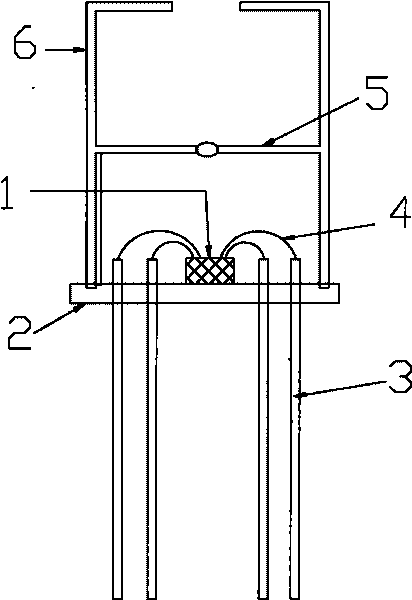
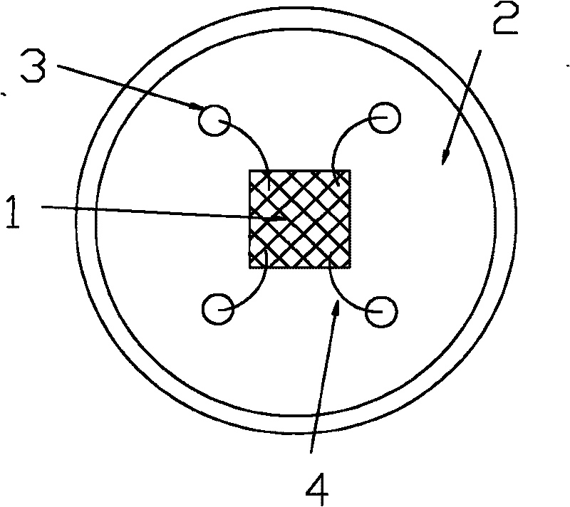
[0028] see figure 1 and 2 , the 850nm photoelectric single-chip integrated receiving chip 1 is pasted on the tube base 2, the pad of the chip is connected to the pin 3 with 4 gold wires 4 by bonding machine, and the tube cap 5 is covered by a capping machine. After completion, it is coaxially packaged with the light-receiving component adapter 6 by laser welding to form a light-receiving component for 100-megabit 850nm optical communication.

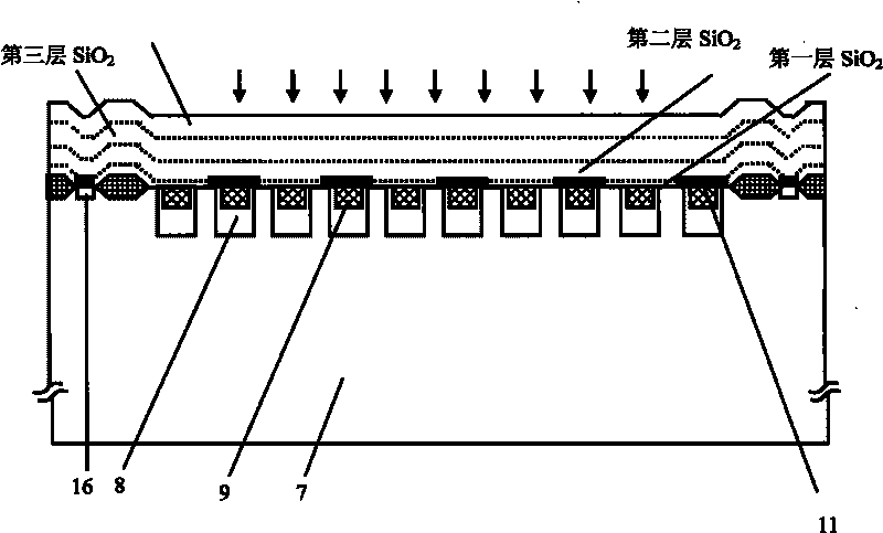
[0029] The 850nm optoelectronic single-chip integrated receiving chip in the present invention adopts a standard CMOS process of 0.5 μm, and is delivered to a foundry through the layout for preparation. The specific preparation method of the silicon photodetector is combined with image 3 and 4 Elaborated as follows:

[0030] First, a P-type silicon wafer is used as the substrate 7; 10 P-well regions 8 with a thickness of about 2.5 μm are realized by ion implantation on the P-type substrate; + region, realize 10 N in 10 P well regio...


PUM

PropertyMeasurementUnit
Widthaaaaaaaaaa
Lengthaaaaaaaaaa

Abstract

The invention relates to an optical receiving assembly for hundred trillion-grade 850nm optical communication and a preparation method thereof, and provides an optical receiving assembly for hundred trillion-grade 850nm optical communication, which is compatible with a commercial CMOS process and can replace the hybrid integration in the traditional 850nm optical transceiver and meet the transmission requirement, and a preparation method thereof. The optical receiving assembly is provided with a 850nm optoelectronic single integrated receiving chip, a pipe seat, a pipe cap, a pipe pin and an adapter, wherein the chip is provided with a prepositive amplifying circuit and an optoelectronic detector, and the prepositive amplifying circuit is provided with two mutual resistance type amplifying circuits, a three-grade differential amplifier, an output buffer circuit and a direct current negative feedback circuit. The optoelectronic detector is provided with a low doped P-shaped silicon substrate, a P pit, an N-shaped heavy doping silicon layer, a field oxide layer, an aluminum layer, three SiO2 insulating medium layers and a Si3N4 surface passivating layer from bottom to top in the longitudinal direction. The chip is attached to the pipe seat by a CMOS process; a welding disk of the chip is bonded with the pipe pin by a gold thread; and the pipe cap is covered to be encapsulated with the adapter according to the same shaft.

Description

technical field [0001] The present invention relates to a receiver optical sub-assembly (ROSA), in particular to a 10M / 100Mbps optical transceiver used for 850nm wavelength communication in an optical fiber access network, for 100-megabit 850nm optical communication Light-receiving components and preparation methods thereof. Background technique [0002] The access network is the bridge connecting the optical fiber backbone network and the user or user premise network, and is the implementation system from the local exchange to the user terminal. At present, the technologies for realizing broadband access network mainly include: Asymmetrical Digital Subscriber Line (Asymmetrical Digital Subscriber Line, ADSL), fiber-coaxial hybrid network (Hybrid Fiber Coax, HFC), wireless access technology, high-speed Ethernet technology and optical fiber access technology etc. Among them, the optical fiber access network combined with the mature campus LAN technology can provide 10M / 100M...

Claims


Application Information

Patent Timeline
IPC IPC(8): G02B6/42H01L23/48H01L21/60
CPCH01L2224/49171H01L2224/48091H01L2924/30111
Inventor 程翔陈朝颜黄苹李继芳
Owner XIAMEN UNIV
Why Eureka
Try Eureka