Thick film photoresist detergent
A cleaning agent and photoresist technology, applied in the field of cleaning agents, can solve the problems of high corrosion of semiconductor wafer patterns and substrates, low corrosion of wafer patterns and substrates, and insufficient cleaning ability, so as to inhibit corrosion dark spots and improve Cleaning ability, low corrosion effect
Inactive Publication Date: 2010-06-16
ANJI MICROELECTRONICS (SHANGHAI) CO LTD
View PDF6 Cites 4 Cited by
- Summary
- Abstract
- Description
- Claims
- Application Information
AI Technical Summary
Problems solved by technology
[0009] The technical problem to be solved by the present invention is that the present invention has overcome existing traditional photoresist cleaning agent to photoresist especially negative photoresist cleaning ability is insufficient, or because operating temperature is higher during cleaning, to semiconductor wafer pattern and Corrosion of the substrate is relatively high and other defects, and a thick-film photoresist that can remove metals, metal alloys or dielectrics, etc. Metal and non-metallic materials such as silicon dioxide have very low corrosion, which makes them show very low corrosion to wafer patterns and substrates. It is a kind of thick film light that is environmentally friendly and can be used in a wide temperature range. Resist cleaning agent
Method used
View moreImage
Smart ImageViewing Examples

Examples
Embodiment 1~25
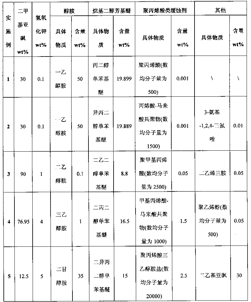
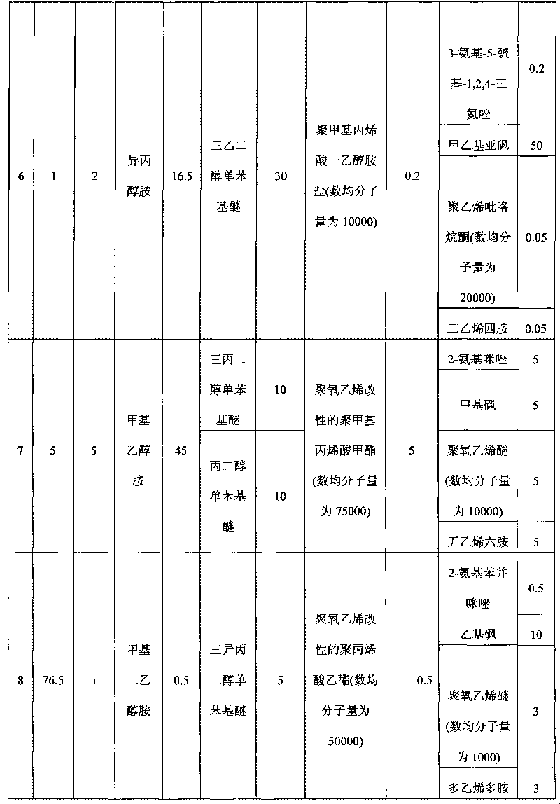
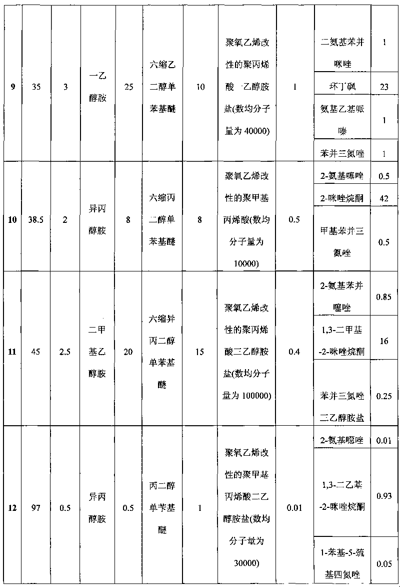
[0033] Table 1 shows Examples 1-25 of the thick-film photoresist cleaning agent of the present invention. According to the components listed in Table 1 and their contents, the cleaning agent of each embodiment can be prepared by simply mixing uniformly.
[0034] Table 1 thick film photoresist embodiment 1~25 of the present invention
[0035]
[0036]
[0037]
[0038]
[0039]
[0040]
Login to View More PUM
| Property | Measurement | Unit |
|---|---|---|
| Thickness | aaaaa | aaaaa |
Abstract
The invention discloses a thick film photoresist detergent, which comprises dimethyl sulfoxide, potassium hydroxide, alcohol amine, alkylene glycol arylene and a polyacrylic acid inhibiter, wherein the number of carbon atoms of alkylene glycol in the alkylene glycol arylene is 3-18. The thick film photoresist detergent can remove thick film photoresist on substrates such as metal, metal alloy or dielectric medium, in particular thick film photoresist with the thickness over 10 mu m, has very low corrosion on metal such as aluminum and copper and nonmetal materials such as silicon dioxide so as to have very low corrosion on wafer patterns and substrates, is environment-friendly and can be used in wide temperature range.
Description
technical field [0001] The invention relates to a cleaning agent in a semiconductor manufacturing process, in particular to a thick-film photoresist cleaning agent. Background technique [0002] In the usual semiconductor manufacturing process, a photoresist mask is formed on the surface of silicon dioxide, copper (Cu) and other metals and low dielectric (k) materials, and then wet or dry etching is used after exposure. Graphic transfer. Thick-film photoresists over 100 μm are increasingly used in semiconductor wafer manufacturing processes, especially thick-film negative photoresists over 100 μm are gradually being used in semiconductor wafer manufacturing processes, and most of the current industrial Photoresist cleaning agents cannot completely remove the negative photoresist with cross-linked network structure after exposure and etching on the wafer, so the cleaning agent used for thick film photoresist has become an important research in the semiconductor wafer manufac...
Claims
Login to View More Application Information
Patent Timeline
 IPC IPC(8): G03F7/42
CPCC11D7/06C11D7/263C11D11/0047G03F7/425H01L21/31133C11D7/34G03F7/426C11D7/3218G03F7/423C11D2111/22
Inventor 史永涛彭洪修曹惠英
Owner ANJI MICROELECTRONICS (SHANGHAI) CO LTD
Features
- Generate Ideas
- Intellectual Property
- Life Sciences
- Materials
- Tech Scout
- Unparalleled Data Quality
- Higher Quality Content
- 60% Fewer Hallucinations
Learn More Browse by: Latest US Patents, China's latest patents, Technical Efficacy Thesaurus, Application Domain, Technology Topic, Popular Technical Reports.
© 2025 PatSnap. All rights reserved.Legal|Privacy policy|Modern Slavery Act Transparency Statement|Sitemap|About US| Contact US: help@patsnap.com