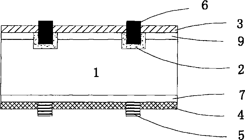
Manufacture method of selective front surface field N-type solar cell
A manufacturing method and a front surface field technology, applied in the field of solar photovoltaic power generation, can solve problems such as electrode difficulties, and achieve the effect of simple process
- Summary
- Abstract
- Description
- Claims
- Application Information
AI Technical Summary
Problems solved by technology
Method used
Image
Examples
Embodiment 1
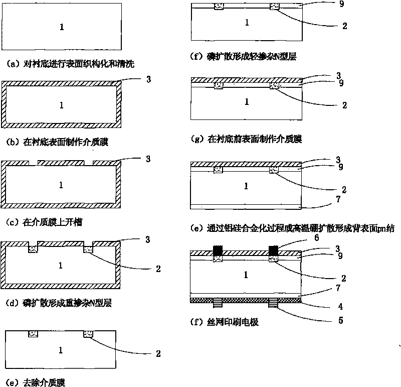
[0053] image 3 It is the first technical solution of the selective front surface field N-type solar cell manufacturing method provided by the present invention, which specifically includes the following steps:
[0054] (a) Surface texturing and chemical cleaning of N-type semiconductor substrates
[0055] For N-type monocrystalline silicon substrates, use dilute sodium hydroxide or potassium hydroxide solution to make a pyramid-shaped light trapping structure on the substrate surface; for N-type polycrystalline silicon substrates, use a mixed solution of nitric acid and hydrofluoric acid on the substrate A pit-like light-trapping structure is made on the surface. Subsequently, the substrate is cleaned with diluted hydrochloric acid and hydrofluoric acid, respectively.
[0056] (b) High-temperature phosphorous diffusion forms a lightly doped N-type layer on the front surface
[0057] Phosphorus oxychloride is used as a dopant source, and the semiconductor substrate is diffu...
Embodiment 2
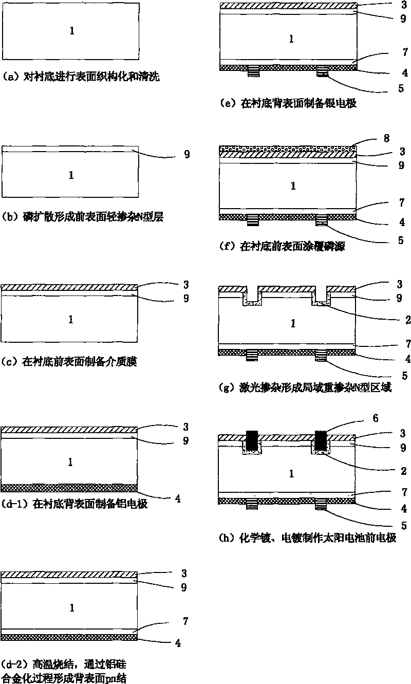
[0073] Figure 4 It is the second technical solution of the selective front surface field N-type solar cell manufacturing method provided by the present invention, which specifically includes the following steps:
[0074] (a) Texturing and chemically cleaning the surface of the N-type semiconductor substrate;
[0075] (b) High-temperature phosphorous diffusion forms a lightly doped N-type layer on the front surface;
[0076] (c) preparing a dielectric film on the front surface of the N-type semiconductor substrate;
[0077] (d) Form a p-type layer on the back surface during the high-temperature boron diffusion process, thereby obtaining a p-n junction on the back surface (using boron tribromide as a doping source, and performing p-type diffusion at a temperature of 800-1000°C);
[0078] (e) preparing silver electrodes and aluminum electrodes by screen printing on the back surface of the N-type semiconductor substrate, and performing high-temperature sintering;
[0079] (f) ...
PUM
 Abstract
Description
Claims
Application Information


