Method for preparing light absorption layer of CIGS (copper indium gallium selenide) thin film solar cell by magnetron sputtering method
A technology for thin-film solar cells and light-absorbing layers, applied in sputtering plating, coatings, circuits, etc., can solve problems such as large differences, changes, difficult control of film uniformity and repeatability, etc., and achieve high-quality and uniform film quality The effect of good performance and simple process
- Summary
- Abstract
- Description
- Claims
- Application Information
AI Technical Summary
Problems solved by technology
Method used
Image

Examples
Embodiment 1
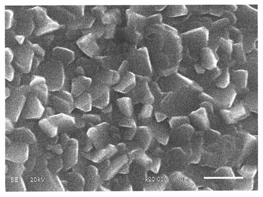
[0042] Preparation of CIGS precursor thin film: on molybdenum-coated soda lime silica glass, with Cu 0.9 In 0.8 Ga 0.2 Se 1.95 As a target, the CIGS precursor film was prepared by radio frequency sputtering, and the sputtering power density was 1.2Wcm -2 , the target distance is 7cm, the working pressure is 1.2Pa; the thickness of the prepared CIGS precursor film is 1200nm, due to the difference of element sputtering rate, in the prepared CIGS precursor film Cu / (In+Ga)=0.86, Ga / (In+Ga) = 0.20.
[0043] Heat treatment of CIGS precursor film: In 30000Pa nitrogen, heat the solid elemental Se source to 230°C to form the saturated vapor pressure of Se, place the CIGS precursor film in the saturated Se vapor pressure, and heat the CIGS at a heating rate of 30°C / min. The precursor film is heated to 530° C. and kept for 30 minutes to prepare the desired CIGS light-absorbing layer.
Embodiment 2
[0045] Preparation of CIGS precursor film: on a molybdenum-coated ceramic plate, with Cu 0.7 In 0.6 Ga 0.4 Se 1.85 As a target, the CIGS precursor film was prepared by radio frequency sputtering, and the sputtering power density was 0.2Wcm -2 , the target distance is 4cm, the working pressure is 0.05Pa; the thickness of the prepared CIGS precursor film is 500nm, due to the difference of element sputtering rate, in the prepared CIGS precursor film, Cu / (In+Ga)=0.67, Ga / (In+Ga) = 0.40.
[0046] Heat treatment of CIGS precursor film: In 100000Pa nitrogen, heat the solid elemental Se source to 180°C to form the saturated vapor pressure of Se, place the CIGS precursor film in the saturated Se vapor pressure, and heat the CIGS at a heating rate of 10°C / min. The precursor film is heated to 450° C. and kept for 60 minutes to prepare the desired CIGS light-absorbing layer.
Embodiment 3
[0048] Preparation of CIGS precursor film: on molybdenum-coated stainless steel foil, with Cu 0.5 In 0.3 Ga 0.7 Se 1.75 As a target, the CIGS precursor film was prepared by radio frequency sputtering, and the sputtering power density was 3.0Wcm -2 , the target distance is 10cm, the working pressure is 5Pa; the thickness of the prepared CIGS precursor film is 1500nm, due to the difference of element sputtering rate, in the prepared CIGS precursor film, Cu / (In+Ga)=0.49, Ga / ( In+Ga) = 0.70.
[0049] Heat treatment of CIGS precursor film: In 10000Pa nitrogen, heat the solid elemental Se source to 350°C to form the saturated vapor pressure of Se, place the CIGS precursor film in the saturated Se vapor pressure, and heat the CIGS at a heating rate of 50°C / min. The precursor film is heated to 500° C. and kept for 30 minutes to prepare the desired CIGS light-absorbing layer.
PUM
| Property | Measurement | Unit |
|---|---|---|
| Thickness | aaaaa | aaaaa |
| Thickness | aaaaa | aaaaa |
Abstract
Description
Claims
Application Information
 - R&D
- Intellectual Property
- Life Sciences
- Materials
- Tech Scout
- Unparalleled Data Quality
- Higher Quality Content
- 60% Fewer Hallucinations
Browse by: Latest US Patents, China's latest patents, Technical Efficacy Thesaurus, Application Domain, Technology Topic, Popular Technical Reports.
© 2025 PatSnap. All rights reserved.Legal|Privacy policy|Modern Slavery Act Transparency Statement|Sitemap|About US| Contact US: help@patsnap.com