MEMS presser sensor chip and manufacturing method thereof

A technology of sensitive chip and pressure, applied in the direction of fluid pressure measurement, manufacturing tools, and manufacturing microstructure devices by changing ohmic resistance, which can solve the problem of long photosensitive effect and hysteresis effect in the electrical connection part of the varistor, and the stress concentration of the varistor. It can solve the problems of low sensitivity and low linearity of the chip, so as to increase the effective bonding area, concentrate the stress area, and improve the sensitivity and linearity.

Inactive Publication Date: 2010-07-14
淮安纳微传感器有限公司
View PDF6 Cites 18 Cited by
  • Summary
  • Abstract
  • Description
  • Claims
  • Application Information

AI Technical Summary

Problems solved by technology

[0004] The existing MEMS pressure-sensitive chip manufacturing method adopts the process of corroding the back cavity first and then forming an electrical connection, which will cause a high fragmentation rate during operation, thereby reducing the yield of the chip; in addition, using the existing

Method used


Image

  • MEMS presser sensor chip and manufacturing method thereof
  • MEMS presser sensor chip and manufacturing method thereof
  • MEMS presser sensor chip and manufacturing method thereof

Examples


Embodiment Construction

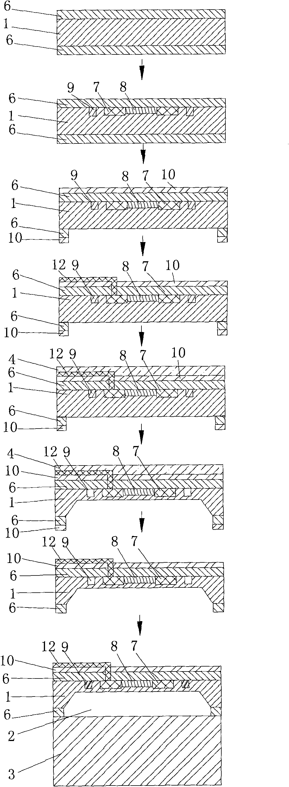
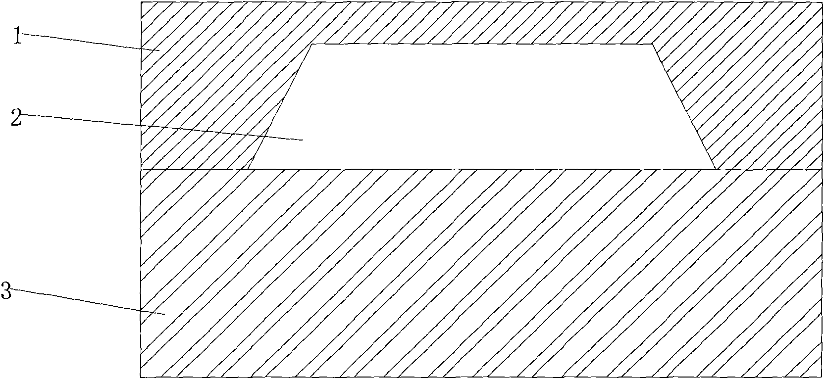
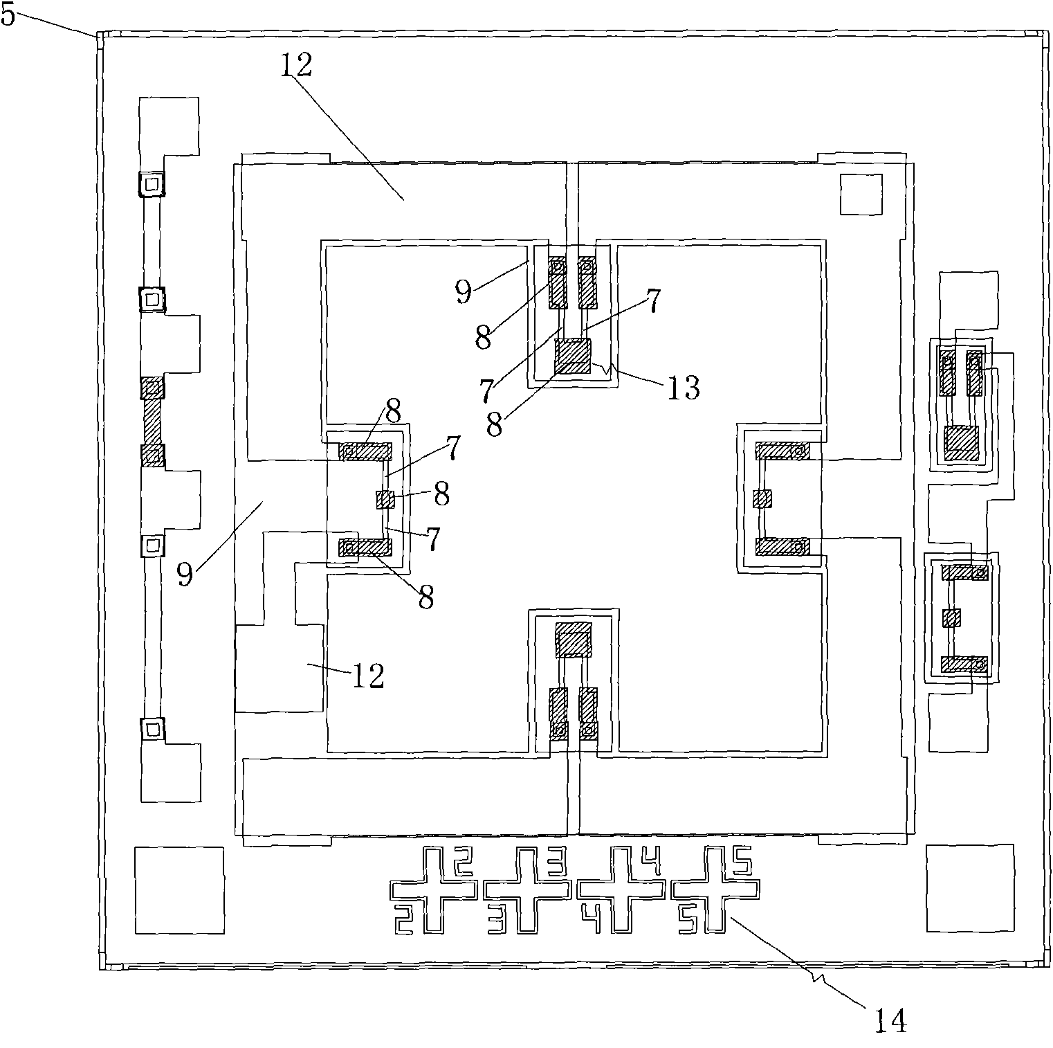
[0029] For the chip structure of the present invention, see figure 2 , image 3 , Which includes a silicon wafer 1, a vacuum chamber 2, a glass substrate 3, a sensitive resistor arrangement area, an external electrical connection member of the sensitive resistor arrangement area, and an alignment mark assembly 14. The four corners of the silicon wafer 1 are respectively provided with alignment marks Structure 5, the maximum stress linear area on the front side of silicon wafer 1 is the sensitive resistor arrangement area, the shape of the sensitive resistor arrangement area is rectangular, and the sensitive resistor arrangement area includes varistor, P + Connection 8, N + Isolation groove 9, aluminum electrode 12, the varistor is specifically two pairs of bridge resistors 13, each of which includes a pair of sensitive resistors 7, which is specifically a linear resistor, and the bridge resistors 13 of each pair of bridge resistors are arranged symmetrically. Arranged on the tw...


PUM


Abstract

The invention relates to an MEMS presser sensor chip, which can effectively improve sensitivity of a chip and enhance yield of the chip. The presser sensor chip comprises a silicon slice, a vacuum cavity, a glass substrate, a sensitive resistor configuration region, an outer electric connecting piece of the sensitive resistor configuration region and an alignment mark component and is characterized in that: the four corners of the positive face and the negative face of the silicon slice are respectively provided with an alignment mark structure; the maximum stress linear region of the positive face of the silicon slice is the sensitive resistor configuration region which is rectangular and comprises a piezoresistor, p+connection, an N+ isolation groove and an aluminum electrode; and the piezoresistor consists of two pairs of bridging resistors concretely, each bridging resistor comprises one pair of sensitive resistors which are linear resistors, each bridging resistor in each pair of the bridging resistors is arranged at two opposite sides of the four sides of the sensitive resistor configuration region respectively in a symmetric manner, and each bridging resistor is encircled by the N+ isolation groove.

Description

(1) Technical field [0001] The invention relates to the field of microelectronic mechanical system (MEMS) pressure sensitive chips, in particular to a MEMS pressure sensitive chip. The invention also relates to a manufacturing method of the chip. (2) Background technology [0002] Micromechanical sensitive devices based on microelectromechanical systems (MEMS) have been widely used and developed rapidly due to their small size, low cost, simple structure, and integration with processing circuits. [0003] As the core device of the pressure sensor, the pressure sensitive chip is the earliest commercial product in the microelectromechanical system (MEMS). The piezoresistive sensitive chip has been more and more widely used due to its large output signal and simple signal processing. There are many important applications for atmospheric pressure detection, such as predicting weather changes and measuring altitude. For pressure sensitive devices that detect atmospheric pressure, the w...

Claims


Application Information

Patent Timeline
IPC IPC(8): G01L9/06B81B7/02B81C1/00B81C3/00
Inventor 王树娟周刚陈晓亮陈会林郭玉刚
Owner 淮安纳微传感器有限公司
Why Eureka
Try Eureka