Micro molecular white-light organic light-emitting device produced by wet method

An electroluminescent device and small molecule technology, which is applied in the direction of electric solid-state devices, electrical components, semiconductor devices, etc., can solve the problems of low purity and low performance of polymer materials, and achieve high cost and stable white light emission in the evaporation process , the effect of easy large-area preparation

Inactive Publication Date: 2010-07-14
XI AN JIAOTONG UNIV +1
View PDF0 Cites 8 Cited by
  • Summary
  • Abstract
  • Description
  • Claims
  • Application Information

AI Technical Summary

Problems solved by technology

In the past, researchers' research on the application of wet-film-making technology basically revolved around polymer materials. There were few reports on wet-film-making small molecule devices. The lifetime and efficiency of WOLEDs based on polymer materials have been continuously improved through efforts, but Compared with vacuum-evaporated small molecule white light devices, there is still a big gap, in which the purity of the polymer material is low, and defects in the chain are one of the reasons for the low performance

Method used


Image

  • Micro molecular white-light organic light-emitting device produced by wet method
  • Micro molecular white-light organic light-emitting device produced by wet method
  • Micro molecular white-light organic light-emitting device produced by wet method

Examples


preparation example Construction

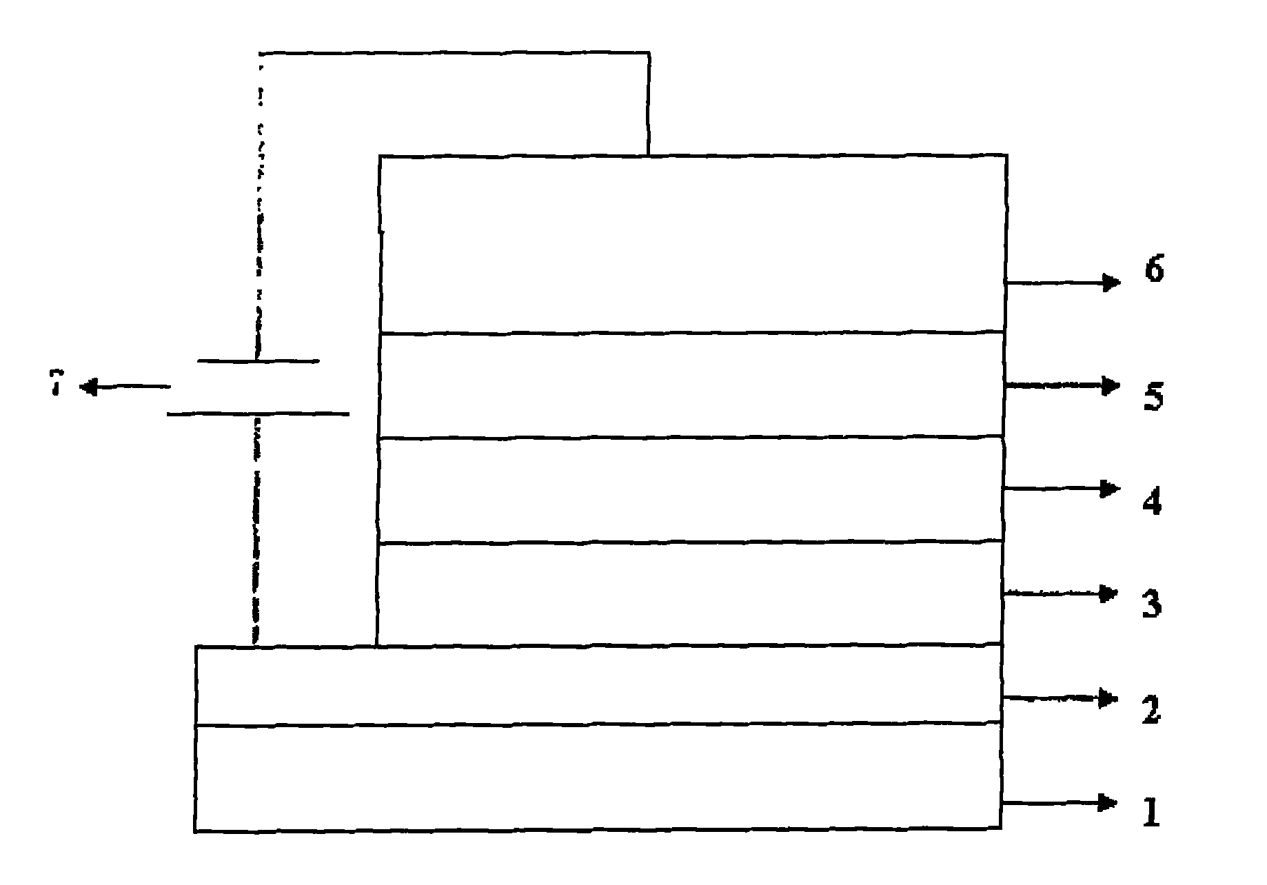
[0036] (3) Preparation of each organic functional layer: put the spin-coated and dried substrate into the vacuum chamber, and sequentially evaporate the hole blocking material to form the hole blocking layer 4. The evaporation rate of the material film 0.01-0.5nm / s, the film thickness is 10-40nm; the organic electron-transporting layer 5 is formed by evaporating an organic electron-transporting material on the hole-blocking layer, the evaporation rate is 0.01-0.5nm / s, and the film thickness is 30-40nm. 40nm.

[0037] (4) Preparation of the cathode 6: keep the pressure in the vacuum chamber constant, and vapor-deposit the LiF / Al composite cathode on the electron transport layer 5 above.

Embodiment 1

[0039] now refer to figure 1 , the electroluminescent device according to the first embodiment of the present invention has the following structure:

[0040]Glass (plastic) substrate / ITO(100nm) / NPB:DPVBi(15wt%):DPAVBi(4%):Rubrene(0.3%)(50nm) / BCP(10nm) / Alq 3 (30nm) / LiF(0.6nm) / Al(80nm)

[0041] (1) Cleaning of glass substrates pre-engraved with ITO: use hot detergent ultrasonic and deionized water ultrasonic methods to clean the transparent conductive substrate ITO glass, and place it under an infrared lamp to dry after cleaning. The ITO film on the substrate is used as the anode layer of the device. The sheet resistance of the ITO film is 5Ω~100Ω, and the film thickness is 80~280nm.

[0042] (2) White light emitting layer: Place the above-mentioned cleaned and dried ITO glass on a KW-4A glue homogenizer, spin-coat the configured mixed solution to form a film by static batching method, and the speed of the glue homogenizer is 1000rpm, The time is controlled at 40s; the sample...

Embodiment 2

[0049] now refer to figure 1 , the electroluminescent device according to the second embodiment of the present invention has the following structure:

[0050] Glass (plastic) substrate / ITO(100nm) / NPB:MADN(15wt%):DPAVBi(5%):Rubrene(0.3%)(50nm) / BCP(10nm) / Alq 3 (30nm) / LiF(0.6nm) / Al(80nm)

[0051] (1) The cleaning of the glass substrate that is engraved with ITO in advance: refer to the corresponding process of embodiment 1;

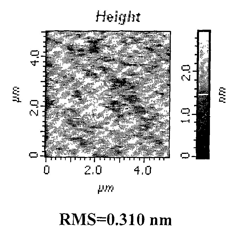
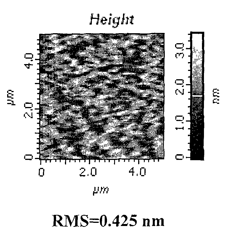
[0052] (2) Mixed white light emitting layer: the optimized ratio of MADN is 15wt%, the optimized doping concentration of blue light dye is 5wt%, and the concentration of yellow light dye is 0.3wt%. The solvent is chlorobenzene, and the spin-coating and drying conditions refer to the corresponding process of Example 1; Figure 2(b) is an AFM image of the surface morphology of the spin-coated organic small molecule hole injection layer, RMS=0.425nm.

[0053] (3) Preparation of each organic functional layer: refer to the corresponding process of Example 1;

...


PUM


Abstract

The invention discloses a micro molecular white-light organic light-emitting device produced by a wet method, the structure of which is a substrate / an anode / hole transport material: a blue-light main body: a blue fluorescent material: a complementary color fluorescent dye / a hole barrier layer / a teleportation layer / an cathode, wherein blue light is emitted by an efficient blue-light host-guest system, a complementary color luminous component is provided by the efficient fluorescent dye, and a luminescent layer adopts a spin coating method to mix an efficient blue-light host-guest material and the fluorescent dye into the hole transport materials to form a single luminescent layer. The device has simple structure, is dispensed with a hole transport layer of a micro molecular evaporation multilayer device, and merges a blue-light emission layer and a yellow-light emission layer into one layer; the device has high brightness, and the white light thereof has pure chromaticity which is reduced along with the variation of the applied driving voltage; and the device has the characteristics of simple preparation technology and low cost. The device can satisfy the requirements of LCDs on light, thin and low consumption, and is very suitable for being used as the backlight of display devices and for common illumination.

Description

technical field [0001] The invention relates to the technical field of organic electroluminescence, and relates to the realization of a small molecule white light organic electroluminescence device prepared by a solution method, so as to simplify the structure of the device, reduce the manufacturing cost, and realize a high-efficiency device with stable color to meet the general lighting requirements. And LCD backlight needs. Background technique [0002] Organic electroluminescence (OLED) is one of the high-tech developed in recent years. It has the advantages of self-luminescence, ultra-thin, low driving voltage, fast response speed, and wide viewing angle. Early organic electroluminescent devices showed potential advantages in flat panel display applications. After nearly two decades of development, OLED display technology has become increasingly mature. Display panels with low information capacity have been applied to mobile phones, MP3, instrument panels and other field...

Claims


Application Information

Patent Timeline
Patent Type & Authority Applications(China)
IPC IPC(8): H01L51/50
Inventor 吴朝新王栋东张新稳侯洵
Owner XI AN JIAOTONG UNIV
Why Eureka
Try Eureka