Design for testability circuit and method for full digital switched capacitor sigma-delta modulator

A technology for switching capacitors and designing circuits, applied in analog/digital conversion calibration/testing, delta modulation, instruments, etc.

Inactive Publication Date: 2010-07-21
PEKING UNIV +1
View PDF0 Cites 12 Cited by
  • Summary
  • Abstract
  • Description
  • Claims
  • Application Information

AI Technical Summary

Problems solved by technology

However, when a digital excitation source is used in the prior art, an analog gain module needs to be used, which will affe

Method used


Image

  • Design for testability circuit and method for full digital switched capacitor sigma-delta modulator
  • Design for testability circuit and method for full digital switched capacitor sigma-delta modulator
  • Design for testability circuit and method for full digital switched capacitor sigma-delta modulator

Examples


Embodiment 1

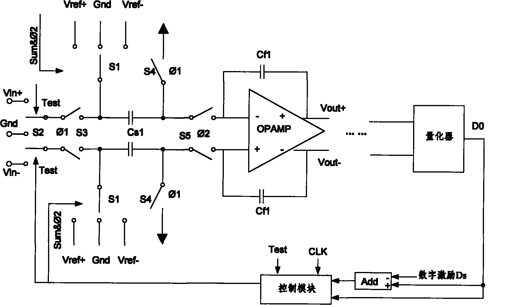
[0045] The circuit feature of the common capacitor mode is that the input sampling capacitor and the DAC feedback capacitor are the same capacitor. The modified circuit using the DFT design of the present invention is as follows: figure 1 shown. The original first-stage integrator includes four groups of switches S1, S3, S4, and S5, capacitors Cs1, Cf1, and an operational amplifier OPAMP. The original integrator used a differential input structure, including Vin+ and Vin-; differential output, including Vout+ and Vout-. The original reference levels are Vref+ and Vref-. and It is a two-phase non-overlapping clock. The DFT method provided by the present invention modifies the first-stage integrator, and other integrator structures and operation timing remain unchanged. The modified first-stage integrator adds a switch S2, the switch S1 is modified from a two-way switch to a three-way switch, and a GND input terminal and a GND reference voltage are added. At the same tim...

Embodiment 2

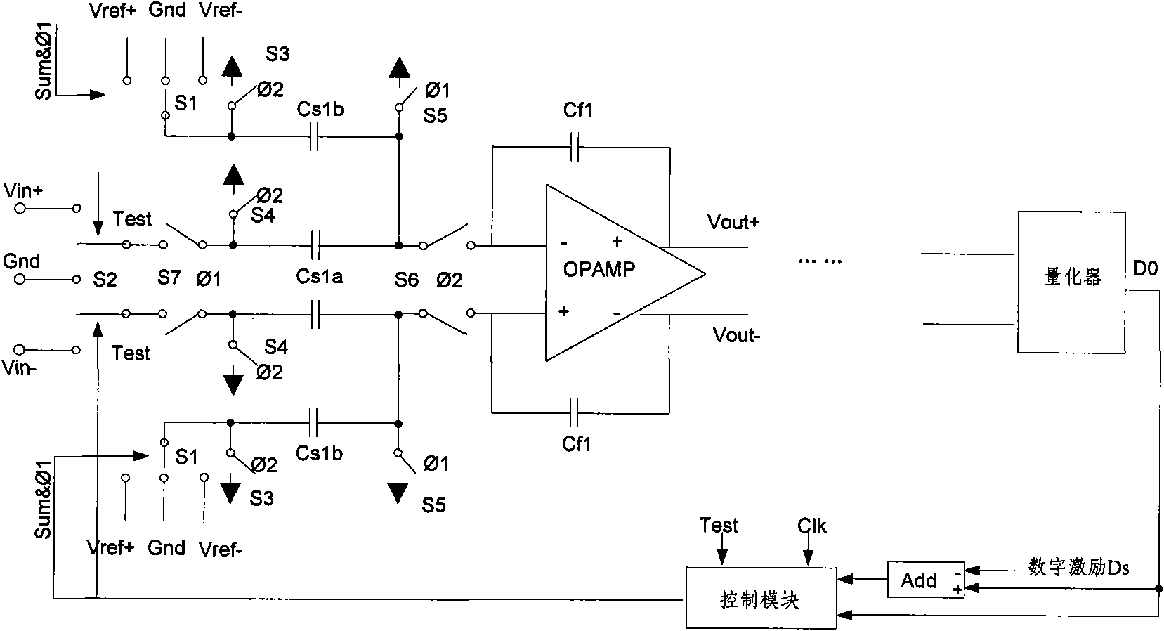
[0047] The circuit feature of the dual-capacitor mode is that the input capacitor and the DAC feedback capacitor are two capacitors. The modified circuit using the DFT design of the present invention is as follows: figure 2 shown. The original first-stage integrator includes six groups of switches S1, S3, S4, S5, S6, and S7, capacitors Cs1a, Cs1b, Cf1, and an operational amplifier OPAMP. The original integrator used a differential input structure, including Vin+ and Vin-; differential output, including Vout+ and Vout-. The original reference levels are Vref+ and Vref-. and It is a two-phase non-overlapping clock. The DFT method provided by the present invention modifies the first-stage integrator, and keeps other integrator structures and operation sequences unchanged. The modified first-stage integrator adds a switch S2, the switch S1 is modified from a two-way switch to a three-way switch, and a GND input terminal and a GND reference voltage are added. At the same t...

Embodiment 3

[0051] The present invention is further described below by taking a second-order common capacitance sigma-delta modulator as an example.

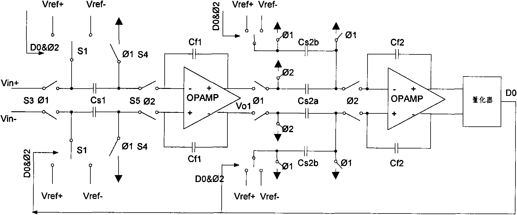
[0052] First design a sigma-delta modulator that meets the requirements, such as image 3 shown. The designed first-stage integrator operation timing is: In the clock phase, switches S3 and S4 are closed, and S1 and S5 are open; In the clock phase, switch S5 is closed, S3 and S4 are open, when D0=1, S1 is connected to Vref+, and when D0=-1, S1 is connected to Vref-.

[0053] Figure 4 for image 3 , using the second-order sigma-delta modulator after adding the DFT module in the present invention. relative to image 3 , the modified parts include: adding switch S2 to control the input terminal; changing switch S1 from a two-way switch to a three-way switch; adding a Gnd option to the input signal; adding a Gnd option to the reference level; adding a mode selection signal Test ; Added a control module; added a digital adder module Ad...


PUM


Abstract

The invention relates to a design for testability method for full digital switched capacitor sigma-delta modulator (DFT), comprising the following steps: modifying according the structure of the designed sigma-delta modulator to be measured, and connecting the original input end to Gnd when testing; multiplexing one feedback DAC contained in the sigma-delta modulator to be measured, and reconfiguring the feedback DAC to three output levels Vref+, Gnd and Vref-; deciding the output of the feedback DAC according to the difference of quantizer digital output (D0) and applied digital drive (Ds), and detecting the performance of the sigma-delta modulator to be measured through analyzing digital drive and quantizer digital output. The invention further provides a corresponding DFT circuit. The technical scheme of the invention provides a full digital switched capacitor sigma-delta modulator DFT method without using expensive analog driving source testing modulator, thereby having at-speed testing ability with very low testing cost and very short testing time and is capable of efficiently reducing time-to-market time of products.

Description

technical field [0001] The invention relates to the field of integrated circuit design and testing, in particular to an all-digital sigma-delta modulator DFT (Design For Testability, design for testability) circuit and method. Background technique [0002] With the development of technology and the progress of design methods, more and more analog chips and even radio frequency chips are integrated with digital chips to form SOC (System on Chip, system on chip) chips. The number of tubes of a chip increases rapidly, but the number of pins does not increase accordingly, which increases the difficulty of testing the chip, thereby increasing the testing cost of the chip. For digital chips, the development of scan chain (SCAN) and BIST (Built-In Self Test Technique, built-in self-test) has effectively improved the controllability and observability of the chip. However, there is no major progress in the testability research of analog chips. The analog circuit DFT method based on...

Claims


Application Information

Patent Timeline
IPC IPC(8): H03M3/02H03M1/10G01R31/3163
Inventor 冯建华任建国叶红飞
Owner PEKING UNIV
Why Eureka
Try Eureka