Double-heterojunction MOS-HEMT component

A double heterojunction and device technology, which is applied in semiconductor devices, semiconductor/solid-state device manufacturing, electrical components, etc., can solve problems such as obvious self-heating effect, serious gate leakage current, and excessive threshold voltage, so as to reduce self- Heating effect, reduction of gate leakage current, effect of concentration reduction

Inactive Publication Date: 2010-07-28
SHANGHAI INST OF TECHNICAL PHYSICS - CHINESE ACAD OF SCI
View PDF0 Cites 15 Cited by
  • Summary
  • Abstract
  • Description
  • Claims
  • Application Information

AI Technical Summary

Problems solved by technology

Nevertheless, AlGaN/GaN/InGaN/GaN double heterojunction HEMT devices still have the following disadvantages: 1. The self-heating effec

Method used


Image

  • Double-heterojunction MOS-HEMT component
  • Double-heterojunction MOS-HEMT component
  • Double-heterojunction MOS-HEMT component

Examples


Embodiment

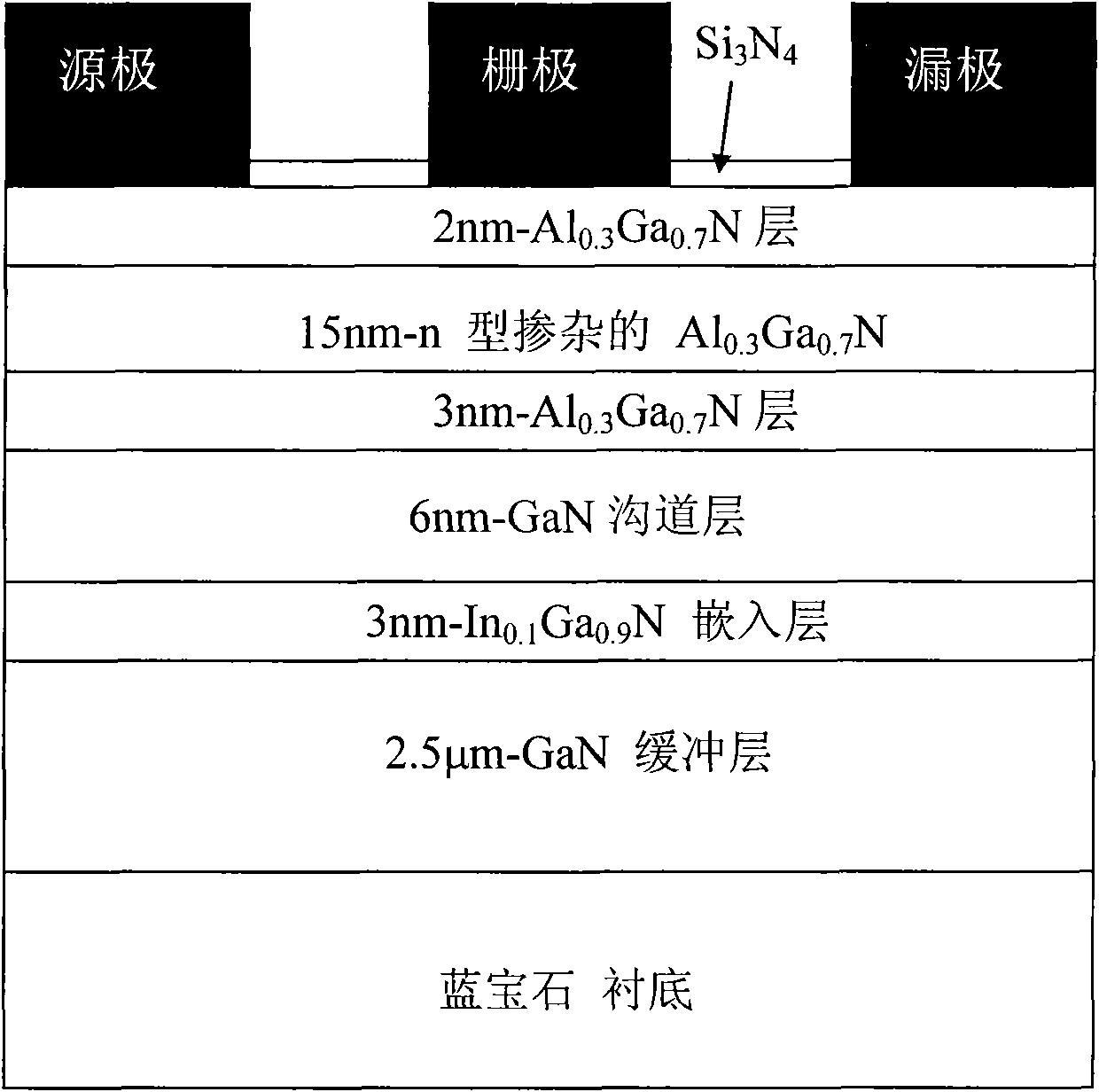
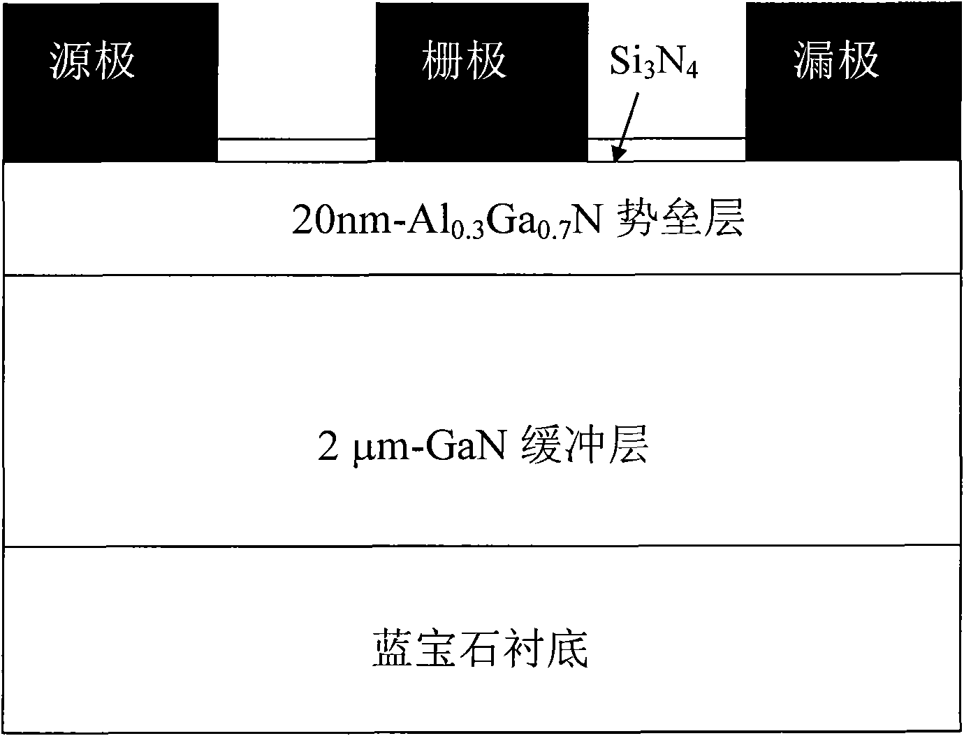
[0056] The present invention simulates Al 2 o 3 / AlN / GaN / InGaN / GaN double heterojunction MOS-HEMT devices to demonstrate their advantages, figure 1 It is the structure diagram of the existing AlGaN / GaN / InGaN / GaN double heterojunction HEMT device, image 3 It is a structural diagram of a traditional AlGaN / GaN HEMT device. The difference of the device of the present invention is that the barrier layer is replaced by AlN, and a MOS structure is adopted. exist Figure 4 We schematically draw the conduction band energy distribution diagrams of these three devices. It can be seen that due to the reverse polarization of the InGaN layer, the existing double heterojunction HEMT device and the double heterojunction MOS- The conduction band energy of the buffer layer of the HEMT device is significantly higher than that of the traditional GaN-based HEMT device, thereby greatly reducing the leakage current of the buffer layer and the current collapse effect. from Figure 4 It can be s...


PUM

PropertyMeasurementUnit
Thicknessaaaaaaaaaa
Thicknessaaaaaaaaaa
Thicknessaaaaaaaaaa

Abstract

The invention discloses a double-heterojunction MOS-HEMT (metal oxide semiconductor-high electron mobility transistor) component comprising a GaN nucleating layer 9, a GaN buffer layer 8, an InGaN embedding layer 7 and a GaN channel layer 6 which are sequentially formed on a sapphire substrate 10, an AlN barrier layer 5 and an Al2O3 gate dielectric layer 4, a source electrode 1 and a drain 3 formed on the AlN barrier layer 5, and a gate electrode 2 formed on the Al2O3 gate dielectric layer 4, wherein the double-heterojunction MOS-HEMT component is characterized in that an AlN material having good heat conductivity and larger band gap is used as the barrier layer, thus reducing the self-heating effect and gate leakage current of the component and reducing the threshold voltage of the component working in a depletion mode; by using the AlN material having strong polarizability, the invention can increase the electron concentration in the channel and increase the output power of the saturation current and the component; by using the Al2O3 material deposited on the basis of the atomic layer deposition process as the gate dielectric layer, the invention can greatly reduce the gate leakage current and increase the breakdown voltage of the component; and by using the reverse polarization of the InGaN material, the invention can increase the conduction band energy of the buffer layer and reduce the current collapse effect of the component.

Description

technical field [0001] The present invention relates to semiconductor component technology, specifically refers to an Al 2 o 3 / AlN / GaN / InGaN / GaN double heterojunction MOS-HEMT devices. Background technique [0002] The third-generation wide-bandgap semiconductor device represented by gallium nitride (GaN) is a new type of wide-bandgap semiconductor device developed rapidly in the past ten years after the first and second-generation semiconductor devices. Since the 1990s, with a series of major breakthroughs in the growth process of gallium nitride (GaN)-based semiconductor materials, a new generation of semiconductor materials represented by GaN has gradually attracted people's attention. It has a large band gap, high electron mobility, High thermal conductivity, with the characteristics of high pressure resistance, thermal decomposition resistance, corrosion resistance and radiation resistance, especially suitable for the production of ultra-high frequency, high temperat...

Claims


Application Information

Patent Timeline
IPC IPC(8): H01L29/778H01L29/78H01L21/336H01L29/205H01L29/51
Inventor 胡伟达王林王晓东陈效双陆卫
Owner SHANGHAI INST OF TECHNICAL PHYSICS - CHINESE ACAD OF SCI
Why Eureka
Try Eureka