Zinc oxide based film transistor and chip preparing process

A thin-film transistor, zinc oxide-based technology, applied in the field of microelectronics, can solve the problems of reduced reliability, low effective mobility, and rising manufacturing costs, and achieve the effects of improving interface characteristics, avoiding cross-contamination, and improving interface quality

Inactive Publication Date: 2006-11-15
ZHEJIANG UNIV
View PDF0 Cites 11 Cited by
  • Summary
  • Abstract
  • Description
  • Claims
  • Application Information

AI Technical Summary

Problems solved by technology

[0005] However, the biggest disadvantage of α-Si:H TFT is the low effective mobility (2 / V.S), at the same time, due to the relatively narrow bandgap of α-Si (~1.7eV), it is opaque in the visible light range, which is not conducive to improving the brightness of the display, and changes in light or ambient temperature will cause device failure, limiting α-Si :H TFT application range, especially α-Si:H TFT can not be used to make start-up circuit, TFT-LCD needs to configure a dedicated peripheral drive circuit, which increases the manufacturing cost and reduces the reliability
[0006] Replacing α-Si with polysilicon technology, although the effective mobility is expected to be greatly improved, but the growth temperature of polysilicon is as high as 600 ° C, transparent glass can hardly withstand high temperatures above 500 ° C, and the manufacturing cost has increased significantly. The absorption of visible light The problem is not completely resolved
[0007] Manufacturing transparent thin-film transistors with wide-bandgap GaN and SiC semiconductors requires high-temperature growth on semiconductor single-crystal substrates. For example, the growth temperature of GaN is ≥800°C, which cannot be grown on glass, and the manufacturing cost is also high.

Method used


Image

  • Zinc oxide based film transistor and chip preparing process
  • Zinc oxide based film transistor and chip preparing process
  • Zinc oxide based film transistor and chip preparing process

Examples


Embodiment 1

[0041] 1. ITO conductive glass cleaning

[0042] Ultrasonic cleaning of the ITO substrate, first with carbon tetrachloride, then with acetone, then with absolute ethanol, and finally blown dry with nitrogen;

[0043] 2. ITO conductive glass photolithography, making TFT structure device unit graphics

[0044] (1) Coating photoresist on the front of the ITO conductive glass with a thickness of about 0.8-0.9 μm;

[0045] (2) Pre-bake on a hot plate to dry the photoresist, the condition is 70-90°C, and bake for 70-100 seconds;

[0046] (3) Photolithography machine exposure, the exposure time is 20 seconds;

[0047] (4) Immerse in developing solution and develop for 15 seconds to make ITO isolated island structure unit pattern;

[0048] (5) ion etching to remove the bottom film for 30 seconds;

[0049] 3. Corrosion of ITO

[0050] Preparation of corrosion solution HCl: H 2 O: HNO 3 =3:2:1, heating in 50°C water bath, corrosion time 40s~60s;

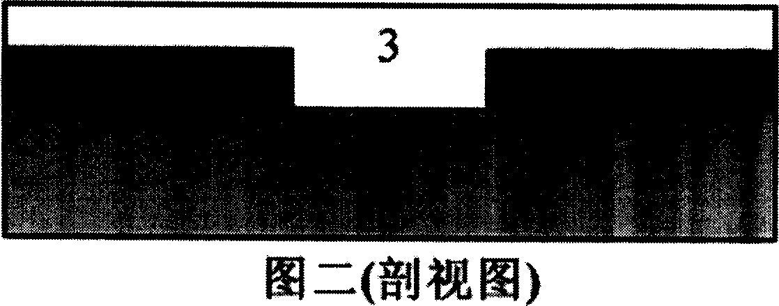
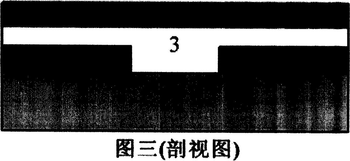
[0051] 4. Epitaxial growth of h...

Embodiment 2

[0076] 1. ITO conductive glass cleaning

[0077] Ultrasonic cleaning of the ITO substrate, first with carbon tetrachloride, then with acetone, then with absolute ethanol, and finally blown dry with nitrogen;

[0078] 2. ITO conductive glass cleaning, photolithography, making TFT structure device unit graphics

[0079] (1) Coating positive photoresist on the front of the ITO conductive glass with a thickness of 0.8-0.9 μm;

[0080] (2) Pre-baking on a hot plate to dry the photoresist at 70-90°C for 70-100 seconds;

[0081] (3) Photolithography machine exposure, the exposure time is 20 seconds;

[0082] (4) Immerse in developing solution and develop for 15 seconds to make ITO isolated island structure unit pattern;

[0083] (5) ion etching to remove the bottom film for 30 seconds;

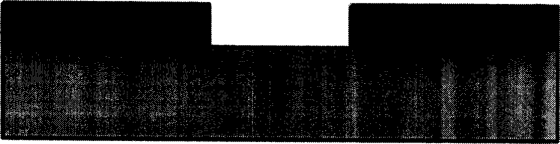
[0084] 3. Corrosion of ITO, see Figure 1

[0085] Preparation of corrosion solution HCl: H 2 O: HNO 3 =3:2:1, 50°C water bath heating, corrosion time 40 seconds to 60 seconds;

[0086] 4. Ep...


PUM

PropertyMeasurementUnit
Thicknessaaaaaaaaaa

Abstract

This invention relates to one application new type high dielectric constant material that cubic ZnMgO crystal film as grid insulating layer, hexagonal phase ZnO base semiconductor nm film as channel layer, ITO or ZnO:Al conducting glass as electrode film TFT reparation technique, it belongs to micro electronic technology field. The advantage is that active layer and grid insulating device structure can grow on the glass substrate to provide one simple TFT manufacture technique, comparing to existing non crystal or multi crystal silicon TFT, the zinc oxide group is transparent to visible light and high mobility. It has great application prospect in flat panel display, printer, and duplicator and video camera products.

Description

technical field [0001] The invention relates to the manufacture of a novel thin-film transistor, which belongs to the technical field of microelectronics, in particular to a zinc oxide-based thin-film transistor and a chip preparation process. Background technique [0002] Thin-film transistor (TFT), also known as thin-film field-effect transistor, is a type of field-effect transistor. Currently, TFT occupies the second largest market for silicon chip technology. It is used in flat panel displays, cameras, printers, copiers and consumer electronics. It is characterized by low cost, because compared with the semiconductor surface treatment, isolation, doping, photolithography, and reduction used in microelectronic devices fabricated on single crystal Si and GaAs substrates, In terms of complex processes such as thin films, the TFT device process is much simpler. The main process is low-temperature deposition of channels and gates on conductive transparent glass substrates and...

Claims


Application Information

Patent Timeline
IPC IPC(8): H01L29/786C23F1/16H01L21/336
Inventor 吴惠桢余萍梁军徐天宁
Owner ZHEJIANG UNIV
Why Eureka
Try Eureka