Ferroelectric oxide/semiconductor composite film diode resistance change memory

A technology of ferroelectric oxide and resistive variable memory, which is applied in the field of microelectronics, can solve the problems of poor reliability of process integration and small number of times of erasing and writing, and achieve the effect of increasing the programming/erasing speed

Active Publication Date: 2010-07-28
FUDAN UNIV
View PDF0 Cites 28 Cited by
  • Summary
  • Abstract
  • Description
  • Claims
  • Application Information

AI Technical Summary

Problems solved by technology

However, the current RRAM of simple oxide materials has a small number of erases and writes, generally less than 10,000 times, and the reliability of process integration is poor.

Method used


Image

  • Ferroelectric oxide/semiconductor composite film diode resistance change memory
  • Ferroelectric oxide/semiconductor composite film diode resistance change memory
  • Ferroelectric oxide/semiconductor composite film diode resistance change memory

Examples


example

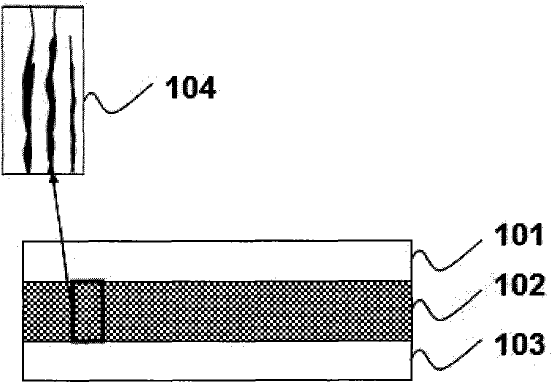
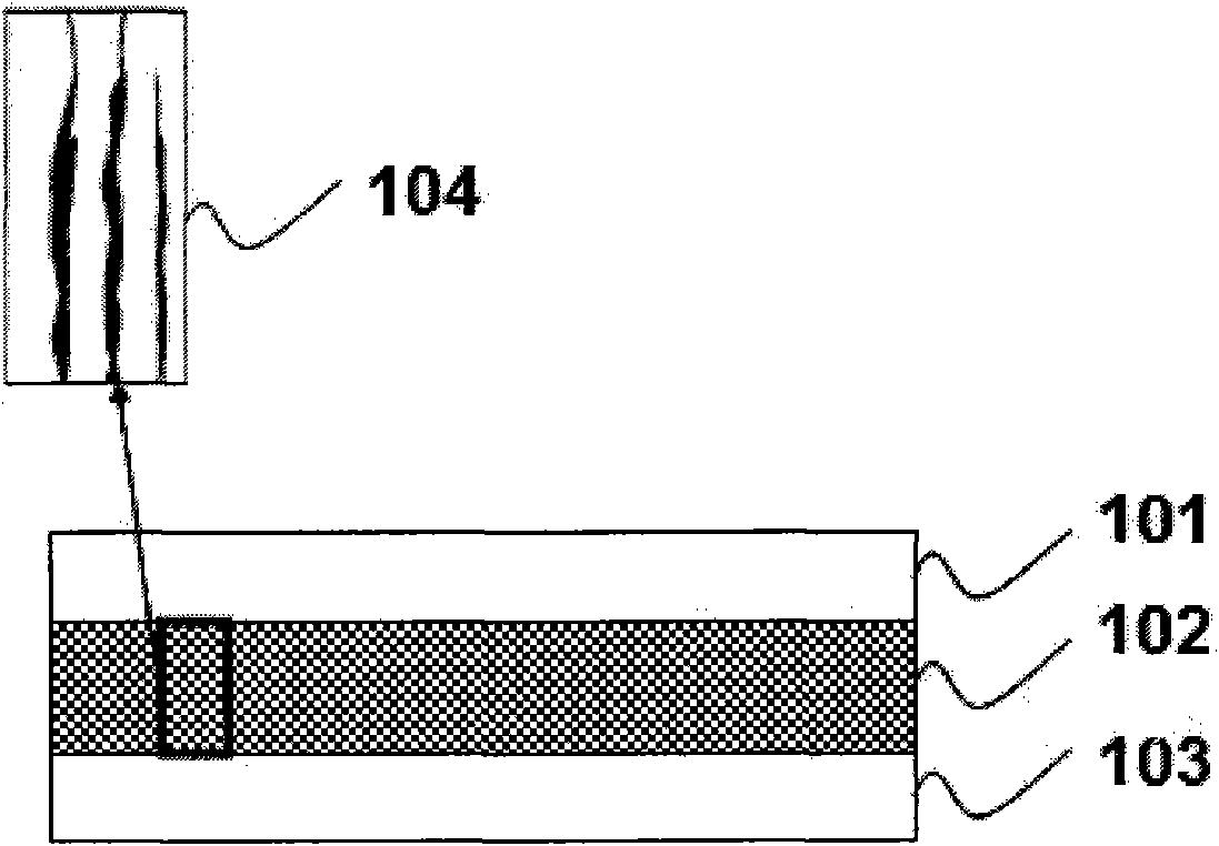
[0027] In this example, the storage unit of the novel ferroelectric oxide / semiconductor compound thin film diode resistive variable memory is as follows: figure 1 As shown, it includes substrate and bottom electrode 103 (strontium ruthenate / strontium titanate), ferroelectric oxide material (bismuth ferrite) / semiconductor (ferrous oxide) composite functional layer 102, top electrode (Pt, Au) 101.

[0028] The above-mentioned device is prepared by the following method:

[0029] 1) With the (100) direction single crystal strontium titanate as the substrate, the bottom electrode of strontium ruthenate (thickness is 10nm-150nm) is grown by pulsed laser deposition (PLD).

[0030] 2) On the above substrate, use PLD to deposit ferroelectric oxide material (bismuth ferrite) / semiconductor (ferric oxide) composite functional layer (thickness is 200nm-500nm), specifically, use trioxide in bismuth ferrite A ceramic target with an excess of 10% ferrous component.

[0031] 3) A platinum m...


PUM

PropertyMeasurementUnit
thicknessaaaaaaaaaa
thicknessaaaaaaaaaa
thicknessaaaaaaaaaa

Abstract

The invention belongs to the technical field of the information memory and particularly relates to a ferroelectric oxide/semiconductor sequentially composite film diode resistance change memory. The resistance change memory comprises a substrate, a bottom electrode, a ferroelectric oxide/semiconductor composite memory function layer and a top electrode, and is prepared by the following method which comprises the following steps: developing compound electrodes, such as strontium ruthenium, lanthanum nickel and the like, or metal on the monocrystal strontium titanate or SiO2/Si substrate to serve as the bottom electrode; then developing the ferroelectric oxide/semiconductor composite film function layer by a pulsed laser deposition or radio frequency magnetron sputtering method; and developing the metal top electrode to form a single diode memory unit structure. The polarity of the diode changes with the orientation of the electric domain. The ferroelectric oxide/semiconductor composite film diode resistance change memory has the advantages of high memory density, good information retentivity and low power consumption.

Description

technical field [0001] The invention belongs to the technical field of microelectronics, and in particular relates to a diode resistive memory with a composite thin film as a functional layer. Background technique [0002] Non-volatile memory is a semiconductor memory that saves information when power is turned off. Its biggest advantage is that the stored data can still be kept for a long time when there is no power supply. At present, flash memory (Flash) is still the mainstream of the non-volatile memory in the market. With the rapid development of digital high-tech, higher requirements are placed on the performance of memory, such as high speed, high density, low power consumption, long life and smaller size. Especially when the feature size of the device is reduced to below 65nm, the contradiction between the erasing speed and reliability of the traditional polysilicon floating gate structure Flash memory device and the leakage of the gate dielectric, etc., the erasing...

Claims


Application Information

Patent Timeline
Patent Type & Authority Applications(China)
IPC IPC(8): H01L45/00G11C11/56
Inventor 江安全王灿刘骁兵
Owner FUDAN UNIV
Why Eureka
Try Eureka