A light-induced infiltration microfluidic chip preparation method and functionalization method

A microfluidic chip and light-induced technology, applied in the fields of biochemistry and microfluidics, can solve the problems of inability to achieve multi-functionality, and achieve the effects of flexible design, reduced production cycle and cost, and reduced preparation cycle

Inactive Publication Date: 2021-01-05
NORTHWESTERN POLYTECHNICAL UNIV
View PDF4 Cites 0 Cited by
  • Summary
  • Abstract
  • Description
  • Claims
  • Application Information

AI Technical Summary

Problems solved by technology

[0003] Can only achieve a specific single function
There have been many related studies on light-induced infiltration, and there are also works on light-driven liquid flow, but they are all based on relatively simple structures, such as capillaries, which cannot achieve multi-functional requirements.

Method used


Image

  • A light-induced infiltration microfluidic chip preparation method and functionalization method
  • A light-induced infiltration microfluidic chip preparation method and functionalization method
  • A light-induced infiltration microfluidic chip preparation method and functionalization method

Examples


Embodiment 1

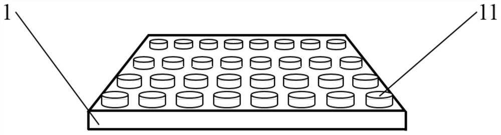
[0045] The preparation of embodiment 1 chip microstructure:

[0046] Clean the quartz chip; spin-coat photoresist on the surface of the 2x2cm quartz chip; pre-bake at 90°C for 10 minutes; use a micro-circular array mask to expose under an ultraviolet light source; remove part of the photoresist with a developer to obtain and Patterns with the same mask shape; post-baking at 150°C for 30 minutes to strengthen the film; use dry etching to obtain a micro-column array with a diameter of 8 microns on the bottom, a diameter of 10 microns on the bottom, a height of 4 microns, and an average column spacing of 3 microns Quartz chip. Such as figure 1 .

[0047] Further, the material of the micropillar array chip 1 includes: glass, quartz, polydimethylsiloxane, polymethyl methacrylate, polycarbonate, polystyrene, polyethylene, polypropylene and the like.

[0048] Further, the shape of the microarray unit 11 includes various shapes such as cylinder, rectangle, triangle, wing, streamlin...

Embodiment 2

[0051] Example 2 Interface modification of light-induced materials

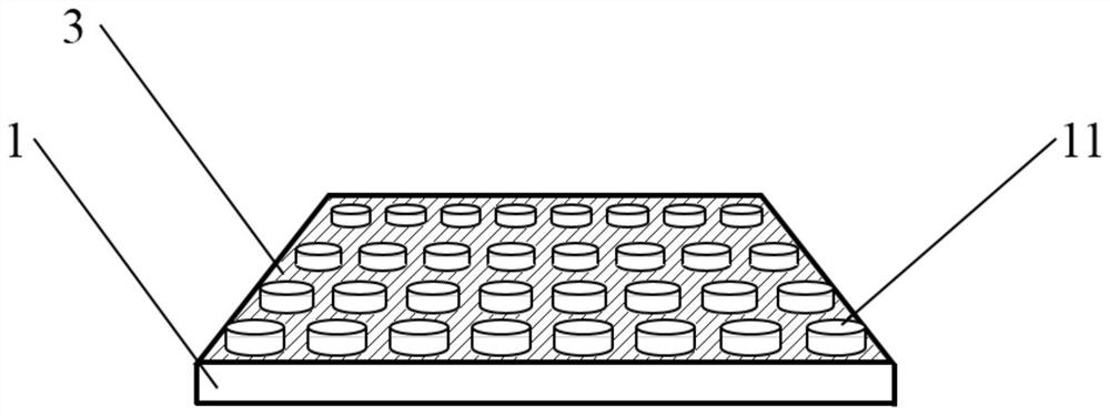
[0052] Use an atomic layer deposition system to deposit a zinc oxide film on the surface of the microarray chip 1 and the flat hole chip 2, such as image 3 and Figure 4 .

[0053] Further, the interface modification materials include organic light-induced materials azobenzenes and spiropyrans, and inorganic light-induced materials such as zinc oxide and titanium dioxide.

Embodiment 3

[0054] Example 3 Response and recovery of light-induced materials

[0055] Contact and seal the coated side of the two chips into a complete chip, such as Figure 5 .

[0056] A photomask 62 is placed between the sealed complete chip and an ultraviolet light source 61 with a wavelength of 365 nm and a light intensity of 145 mW / cm2. Align the chip with the mask and expose for 5 minutes, as Figure 6 . Pure water is injected from the hole at one end of the exposure area to wet the exposure area 63 to form a fluid channel.

[0057] The hydrophobicity of the two chips is restored by heat treatment, black box placement, visible light irradiation, etc., so as to realize the erasure of the fluid channel.

[0058] Various patterns and multifunctional chip functions can be realized through photomask exposure (62), including various microfluidic chip patterns such as linear, cross, H, Y, and Christmas tree shapes. During the exposure process: the wavelength of the ultraviolet light s...


PUM

PropertyMeasurementUnit
lengthaaaaaaaaaa
widthaaaaaaaaaa
widthaaaaaaaaaa

Abstract

The invention relates to a preparation method and a functionalization method of a light-induced infiltration microfluidic chip. The surface of the chip is modified by a light-induced hydrophilic and hydrophobic material, and a hydrophilic and hydrophobic region boundary area is generated in the microstructure by ultraviolet exposure. An infiltration region can allow a fluid to pass through, and the fluid cannot enter a non-hydrophobic region subjected to Laplace pressure between columns, so that microfluidic channels are realized. By use of a photomask, exposure of different designs can be realized inside the chip, and different structures and functions of microfluidic chips are realized. Through the design of pressure-driven fluid channels and electroosmotic flow-driven fluid channels, the microfluidic chip can be erasable and can realize multifunctions on a single chip, and the production cycle and cost of design-fabrication-testing-reprocessing needed by traditional chips can be reduced. All the functions such as separation, synthesis, mixing and flow control of the microfluidic chips can be realized.

Description

technical field [0001] The invention belongs to the field of microfluidic technology and the field of biochemistry, and relates to a preparation method and a functionalization method of a light-induced infiltration microfluidic chip, in particular to a light-induced infiltration multi-chemical biological chip capable of realizing a single chip structure. Enclosed microfluidic chips for analytical functions and their fabrication. Background technique [0002] The basic preparation method of the existing chip is mainly the micromachining technology of glass, hard polymers (such as polycarbonate, polymethyl methacrylate, etc.) and elastic polymers (such as polydimethylsiloxane). Among them, photolithography is the core technology of preparation. Photolithography usually includes three steps of pattern transfer (exposure), development and etching to obtain the designed microstructure on the chip. Some researchers have developed a LIGA high-resolution etching process based on p...

Claims


Application Information

Patent Timeline
Patent Type & Authority Patents(China)
IPC IPC(8): B01L3/00
CPCB01L3/5027B01L3/502707B01L3/50273B01L2200/10B01L2300/0861B01L2300/0887B01L2300/12B01L2300/161
Inventor 谢彦博杨思航段利兵李君杨雅洁
Owner NORTHWESTERN POLYTECHNICAL UNIV
Why Eureka
Try Eureka