Micro fluid control detection device based on surface-enhanced Raman scattering active substrate

A surface-enhanced Raman, active substrate technology, applied in Raman scattering, processes for producing decorative surface effects, electrical solid devices, etc. Cumbersome, restrictions and other issues, to achieve the effect of promoting research and production development, improving production efficiency and integration, and reducing industrial production costs

Active Publication Date: 2010-08-04
PEKING UNIV
View PDF4 Cites 72 Cited by
  • Summary
  • Abstract
  • Description
  • Claims
  • Application Information

AI Technical Summary

Problems solved by technology

However, the monolayer arrangement process of nanospheres is cumbersome, and it is difficult to a

Method used


Image

  • Micro fluid control detection device based on surface-enhanced Raman scattering active substrate
  • Micro fluid control detection device based on surface-enhanced Raman scattering active substrate
  • Micro fluid control detection device based on surface-enhanced Raman scattering active substrate

Examples


Embodiment 1

[0046] Example 1. Preparation of microfluidic detection device based on SERS substrate

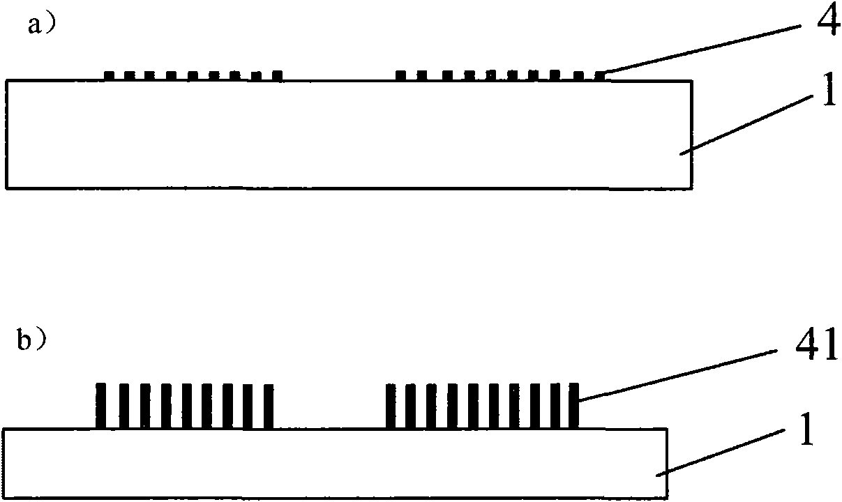
[0047] 1) Preparation of SERS active substrate

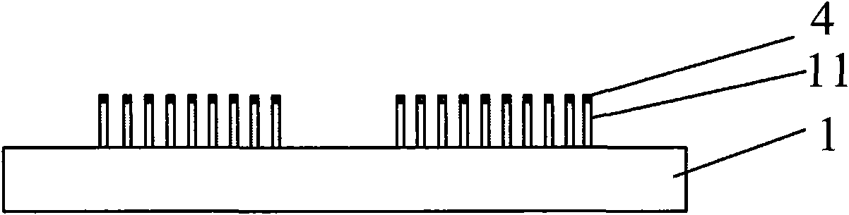
[0048] Spin-coat RZJ-304 positive photoresist with a thickness of 1 μm on the surface of the silicon substrate 1 (substrate a), pre-bake it in an oven at 98°C for 15 minutes, use a wavelength of 365nm, and an intensity of 5.4mW / cm 2 The ultraviolet light is irradiated for 5s through the mask plate, and developed in the developer of RZJ-304 positive photoresist for 30s to form a photoresist pattern in the shape of a microchannel; put the silicon substrate 1 with the photoresist pattern into Power is 250W, oxygen flow rate is in the oxygen plasma bombardment cavity of 30sccm / min, carry out 5 minutes bombardment to photoresist, prepare nanoparticle structure on silicon substrate 1; The silicon substrate with nanoparticle structure 1 Put in a power of 400W, SF 6 and C 4 f 8 In the cavity of a reactive ion etching machine with a flow rate of ...

Embodiment 2

[0051] Example 2. Preparation of microfluidic detection device based on SERS substrate

[0052] 1) Preparation of SERS active substrate

[0053] Spin-coat Shipley SPR positive photoresist with a thickness of 5 μm on the surface of the silicon substrate 1 (substrate a), pre-bake it in an oven at 98°C for 15 minutes, use a wavelength of 365nm, and an intensity of 5.4mW / cm 2 The ultraviolet light is irradiated for 60s through the mask, and developed in the developer of Shipley SPR positive photoresist for 90s to form a photoresist pattern in the shape of a microchannel; the silicon substrate 1 with the photoresist pattern is put into the power In an oxygen plasma bombardment cavity with an oxygen flow rate of 250W and an oxygen flow rate of 30 sccm / min, the photoresist is bombarded for 25 minutes to prepare a nanoparticle structure on the substrate; the silicon substrate 1 with the nanoparticle structure is placed in Power is 400W, SF 6 and C 4 f 8 In the cavity of a reactive...

Embodiment 3

[0055] Example 3. Preparation of microfluidic detection device based on SERS substrate

[0056] 1) Preparation of SERS active substrate

[0057] Spin-coat Shipley AZ series positive photoresist with a thickness of 20 μm on the surface of the silicon substrate 1 (substrate a), and use a wavelength of 365 nm and an intensity of 4.5 mW / cm 2 The ultraviolet light is irradiated through the mask plate for 400s, and developed in the developer of Shipley AZ series positive photoresist for 600s to form a photoresist pattern in the shape of a microchannel; put the silicon substrate 1 with the photoresist pattern into Power is 250W, oxygen flow rate is 30sccm / min oxygen plasma bombardment cavity, carry out 100 minutes bombardment to photoresist, prepare nanoparticle structure on the substrate; Put the silicon substrate 1 with nanoparticle structure The input power is 400W, SF 6 and C 4 f 8In the cavity of a reactive ion etching machine with a flow rate of 40 and 90 sccm / min, the sili...


PUM

PropertyMeasurementUnit
Thicknessaaaaaaaaaa
Thicknessaaaaaaaaaa
Groove depthaaaaaaaaaa

Abstract

The invention discloses a micro fluid control detection device based on surface-enhanced Raman scattering active substrate. The micro fluid control detection device is obtained by the method including the following steps: photoresist is coated on substrate in spinning way, prebaking, exposure, developing and fixing are sequentially carried out on the photoresist, so as to form photoresist graph in micro fluid shape; plasma dry etching is carried out on the photoresist, thus forming nano granular structure or nano fiber upright structure in vertical distribution on the substrate; the nano granular structure is a mask, anisotropic etching is carried out on the substrate, thus forming nano column on the substrate; metal nano granular layer is sputtered on the silicon nano column or nano fiber upright structure, so as to obtain surface-enhanced Raman scattering active substrate; and a silicon-PDMS double-layer structure SERS micro fluid control detection device which has no impurity interference and can be monitored in real time is formed by combining micro fluid device and processing technology thereof. The micro fluid control device not only can be used for detection of liquid analyte to be analyzed but also can be used for detection of colloid and gas analyte to be analyzed.

Description

technical field [0001] The invention relates to a microfluidic detection device based on a surface-enhanced Raman scattering (SERS) active substrate. Background technique [0002] Raman scattering spectroscopy detection is a method of material structure analysis that does not require labeling of the sample to be detected. It is non-destructive and non-contact. With the development of laser technology and weak signal detection and reception technology, Raman scattering spectroscopy detection, as a means of detecting material structure and molecular level, is expected to gain wider and wider recognition in the fields of biological detection, disease diagnosis, environmental monitoring, chemical analysis and so on. practical application. However, due to the small Raman scattering cross-section and the low analytical sensitivity of Raman scattering detection, it is difficult to obtain Raman spectra of many molecules or groups. Although the intensity of the Raman scattering spe...

Claims


Application Information

Patent Timeline
IPC IPC(8): B81C1/00B82B3/00B81B7/00G01N21/65
Inventor 毛海央吴文刚张煜龙黄如郝一龙王阳元
Owner PEKING UNIV
Why Eureka
Try Eureka