Chip design method for multi-chip module of high-performance processor with optical interface

A high-performance processor and multi-chip component technology, applied in the field of computer engineering, can solve problems such as interference and isolation of high-power photoelectric conversion chips MCM chips, and achieve excellent signal integrity guarantee, strong anti-electromagnetic interference ability, and signal transmission characteristics. Good results

Inactive Publication Date: 2010-08-25
NAT UNIV OF DEFENSE TECH
View PDF5 Cites 13 Cited by
  • Summary
  • Abstract
  • Description
  • Claims
  • Application Information

AI Technical Summary

Problems solved by technology

[0014] In the integrated design of high-performance processor MCM chips with optical interfaces, it is necessary to solve the problem of hybrid integration of optical interface pins and electrical interface pins, the hybrid integration of silicon-based semiconductor chips and III-V compound substrate optical devices, Mixed integration of high-speed digital circuits and analog circuits, high-speed signal interference and isolation measures, heat dissipation of high-power photoelectric conversion chips, and sealing and protection of MCM chips, but there is no high-performance processor multi-chip with optical interface that can solve these problems. Component chip design method released

Method used


Image

  • Chip design method for multi-chip module of high-performance processor with optical interface
  • Chip design method for multi-chip module of high-performance processor with optical interface
  • Chip design method for multi-chip module of high-performance processor with optical interface

Examples


Embodiment Construction

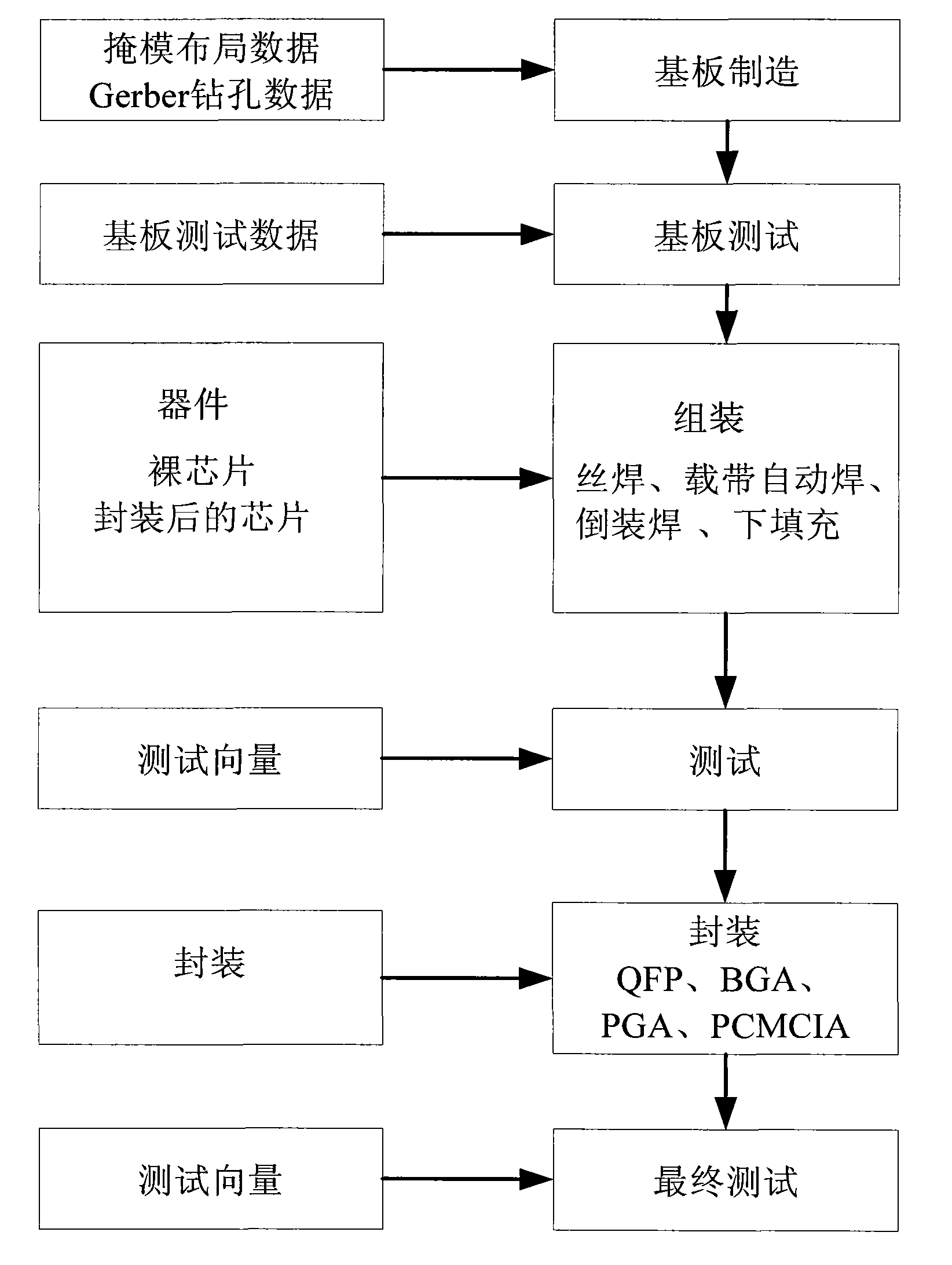
[0059] figure 1 It is the multi-chip module flow chart described in the background technology "MCM Design Manual".

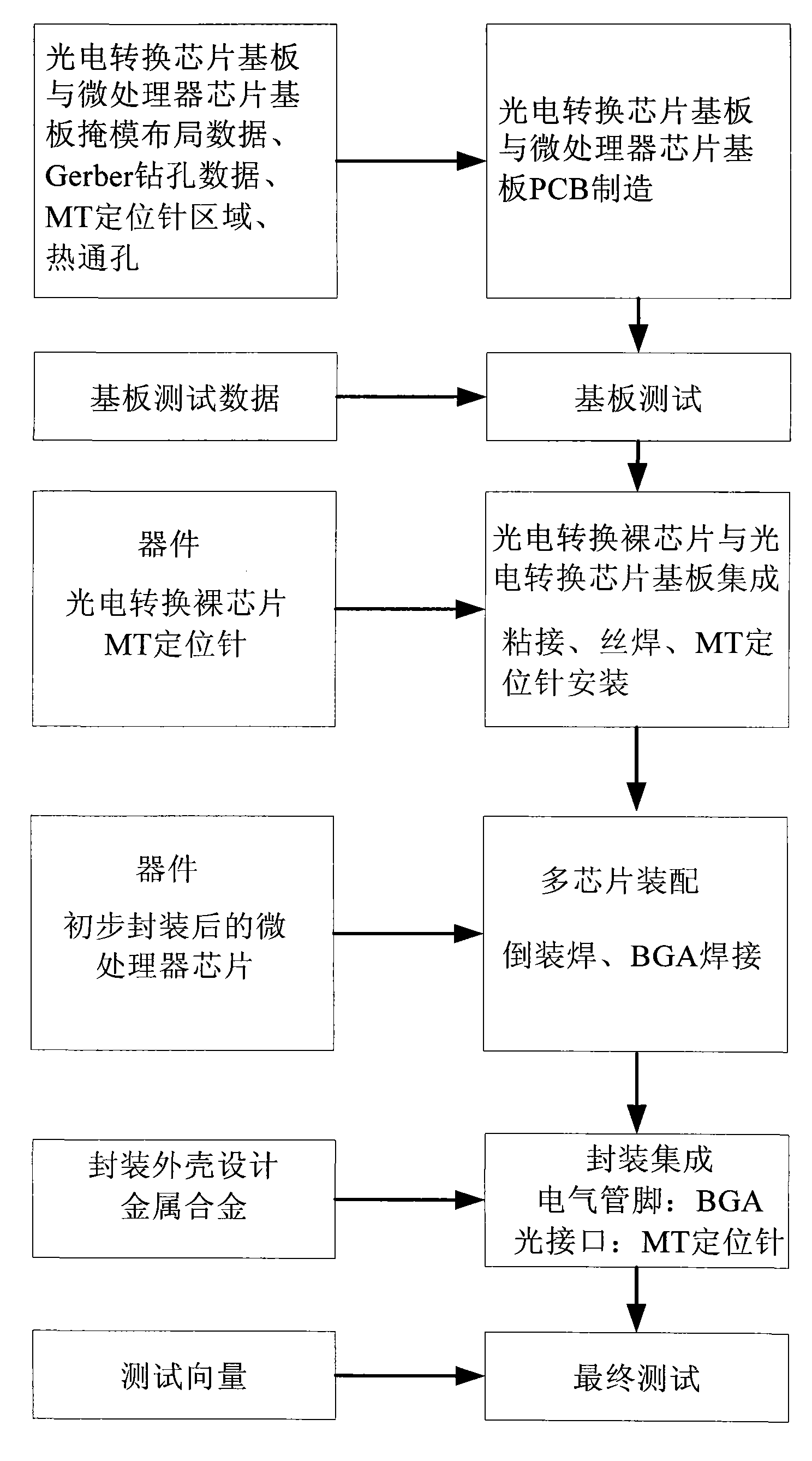
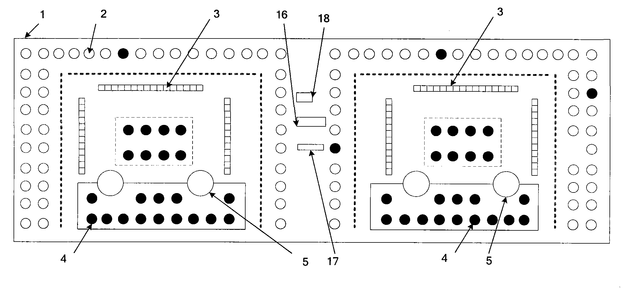
[0060] figure 2 Be the flow chart of the present invention, image 3 It is the PCB block diagram of the photoelectric conversion chip substrate, Figure 4 It is the PCB block diagram of the microprocessor chip substrate, Figure 5 It is a block diagram of a high-performance processor MCM chip with an optical interface prepared by the invention. combine image 3 , Figure 4 , Figure 5 right figure 2 Be explained:

[0061] The first step is to manufacture the photoelectric conversion chip substrate and the microprocessor chip substrate PCB, the method is:

[0062] Such as image 3 As shown, firstly, the photoelectric conversion chip substrate PCB1 is designed by using a high-speed printed circuit board. Wire bonding pads 3 , ball grid array BGA pads 2 and passive device pads are designed on the upper surface of the substrate, including resistor pads ...


PUM


Abstract

The invention discloses a chip design method for a multi-chip module of a high-performance processor with an optical interface so as to solve the problems of the hybrid integration of the optical interface pin based on an MT locating pin with the pin of ball grid array (BGA) of a high-speed electrical interface of the high-performance processor, and the hybrid integration of a high-speed digital circuit with an analog circuit. The invention has the technical scheme that a photoelectric conversion chip substrate and a microprocessor chip substrate PCB are firstly made; a photoelectric conversion bare chip and the photoelectric conversion chip substrate PCB are integrated after testing; then multiple chips are assembled; the microprocessor chip substrate PCB with the multiple chips is encapsulated, thus obtaining an MCM chip; and at last the MCM chip is tested. The invention solves the problem of the hybrid integration of optical and electrical pins, devices and circuits. A chip for the multi-chip module of a high-performance processor can be designed and has high electromagnetic interference resistance and favorable signal transmission characteristic.

Description

technical field [0001] The invention relates to a multi-chip component (Multi-Chip Module, MCM) chip design method in the field of computer engineering, in particular to a design method for a high-performance processor MCM chip with a high-speed optical interface. Background technique [0002] The integration density of integrated circuit chips, the density and speed of I / O pins, and the continuous improvement of chip performance have brought many technical difficulties to the design of integrated circuits and printed circuit boards. The growth rate of chip performance has far exceeded the growth rate of interconnection performance. Traditional inter-chip electrical interconnection has problems such as limited bandwidth, severe crosstalk, and high power consumption, and cannot meet the system application requirements of large-capacity data transmission, new-generation communication equipment, and high-performance computers. The optical interconnection method between chips c...

Claims


Application Information

Patent Timeline
Patent Type & Authority Applications(China)
IPC IPC(8): H01L21/50H01L21/60H01L21/48H01L23/06
CPCH01L2224/73253H01L2924/15311
Inventor 窦文华刘光明冯权友韩岗陈雄斌班冬松杨威
Owner NAT UNIV OF DEFENSE TECH
Why Eureka
Try Eureka