Method for preparing copper-indium-gallium-selenium(sulfur) light absorption layer by adopting non-vacuum process

A technology of copper indium gallium selenide and light absorbing layer, which is applied in the direction of chemical instruments and methods, final product manufacturing, sustainable manufacturing/processing, etc., can solve problems such as inconvenience, and achieve the effect of reducing porosity problems

Inactive Publication Date: 2010-09-01
昆山正富机械工业有限公司
View PDF7 Cites 6 Cited by
  • Summary
  • Abstract
  • Description
  • Claims
  • Application Information

AI Technical Summary

Problems solved by technology

[0010] This shows that above-mentioned existing method for making light-absorbing layer obviously still has inconvenience and defect in method and use, and urgently needs to be further improved
In order to solve the above-mentioned proble

Method used


Image

  • Method for preparing copper-indium-gallium-selenium(sulfur) light absorption layer by adopting non-vacuum process
  • Method for preparing copper-indium-gallium-selenium(sulfur) light absorption layer by adopting non-vacuum process
  • Method for preparing copper-indium-gallium-selenium(sulfur) light absorption layer by adopting non-vacuum process

Examples


Embodiment Construction

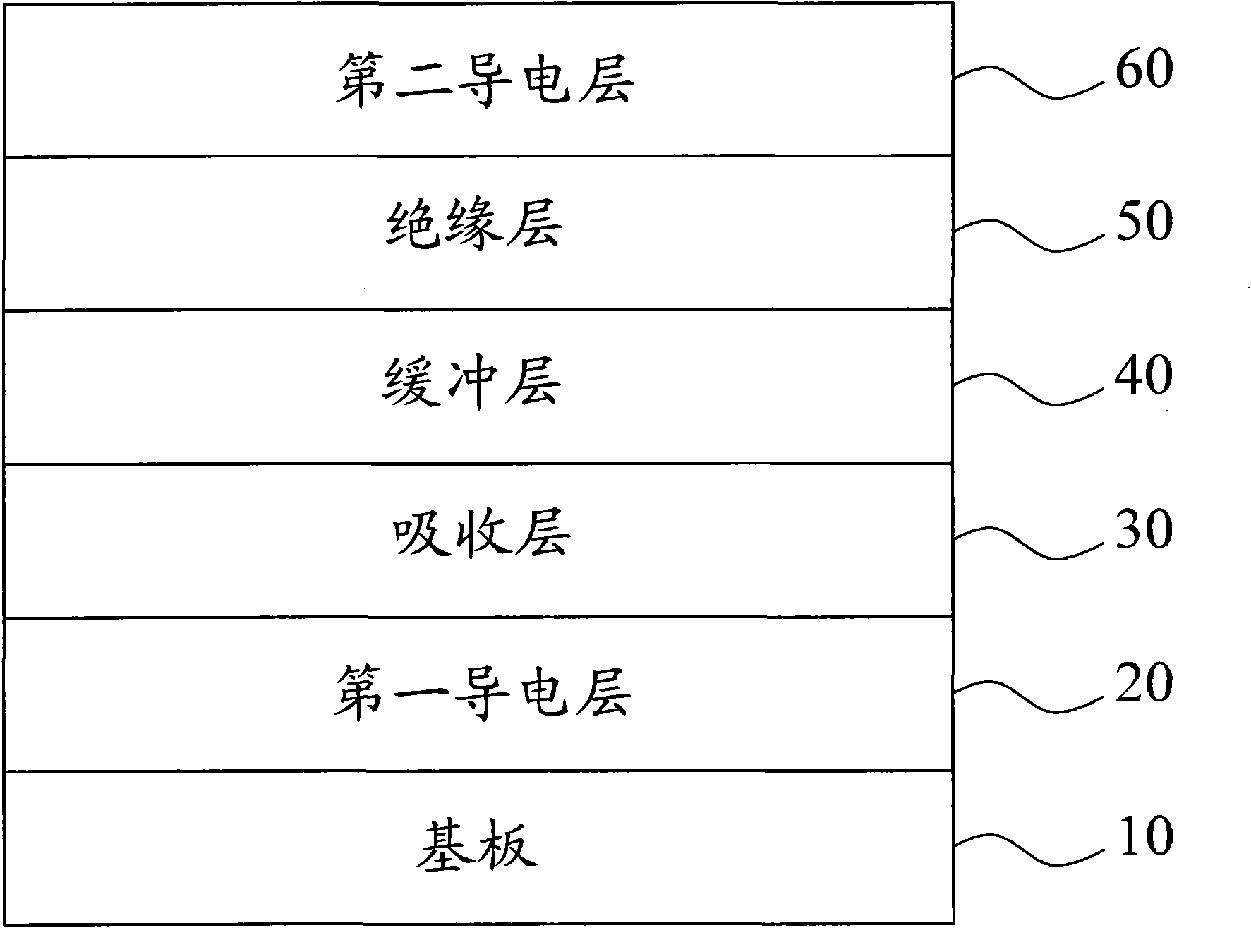
[0041] In order to further illustrate the technical means and effects that the present invention takes to achieve the intended invention purpose, below in conjunction with the accompanying drawings and preferred embodiments, the copper indium gallium selenide (sulfur) light absorbing layer made by non-vacuum process proposed according to the present invention will be described below. The specific implementation, method, steps, features and effects of the method are described in detail below.

[0042] The aforementioned and other technical contents, features and effects of the present invention will be clearly presented in the following detailed description of preferred embodiments with reference to the drawings. For convenience of description, in the following embodiments, the same elements are denoted by the same numbers.

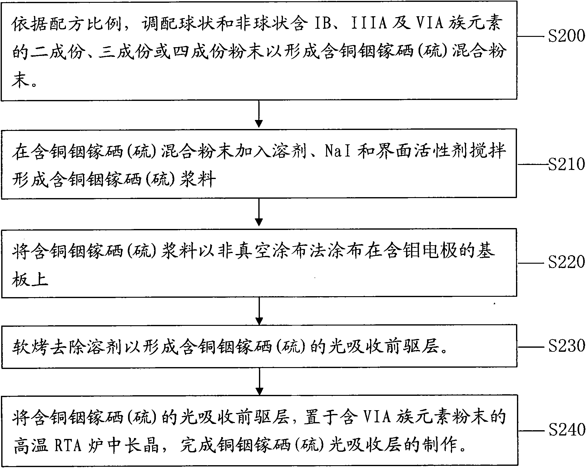
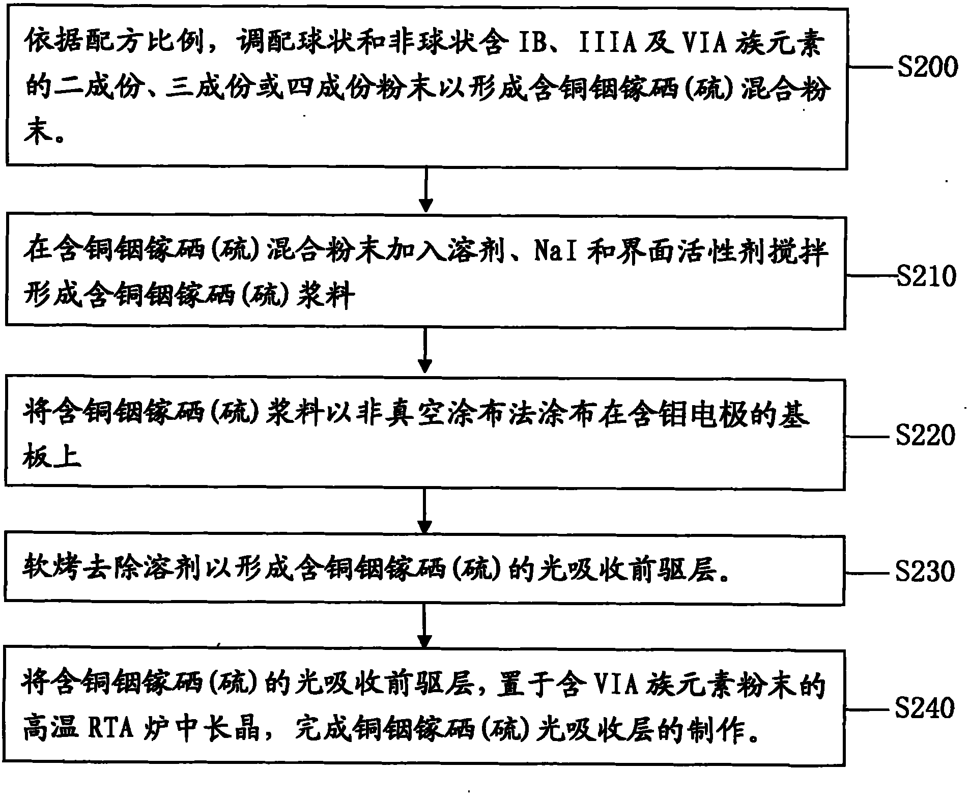
[0043] The present invention mainly uses copper indium gallium selenide or copper indium gallium selenide (sulfur) slurry to be prepared by using differen...


PUM


Abstract

The invention relates to a method for preparing a copper-indium-gallium-selenium(sulfur) light absorption layer by adopting a non-vacuum process. The method comprises the following steps of: in a formula ratio, blending spherical and non-spherical two component powder, three component powder or four component powder containing IB, IIIA and VIA group elements to obtain copper-indium-gallium-selenium(sulfur)-containing mixed powder, wherein the average grain size of the powder is less than 500 nanometers; adding a solvent, NaI and an interface active agent into the copper-indium-gallium-selenium(sulfur)-containing mixed powder, stirring the mixture to obtain copper-indium-gallium-selenium(sulfur)-containing pulp; coating the pulp on a molybdenum electrode-containing substrate by a non-vacuum coating method, obtaining a copper-indium-gallium-selenium(sulfur)-containing light absorption precursor layer by soft-baking; and putting the copper-indium-gallium-selenium(sulfur)-containing light absorption precursor layer in a high-temperature RTA furnace containing VIA group element powder for growing crystals, and obtaining the copper-indium-gallium-selenium(sulfur) light absorption layer. In the method, because the spherical nanometer particles and at least one kind of non-spherical nanometer particles are mixed, the pore problems occurring in the film-forming process are solved; in addition, a selenization method is not adopted, so that the dangerous hydrogen selenide is avoided using.

Description

technical field [0001] The invention relates to a method for making a light absorbing layer, in particular to a method for making a copper indium gallium selenide (sulfur) light absorbing layer by a non-vacuum process. Background technique [0002] In recent years, with the rise of international oil prices and the rise of environmental protection awareness, green energy has become the mainstream of new energy. Among them, solar cells are obtained from the stable radiation energy of the sun, and the source will not be exhausted. Funding and policy subsidies are used to support the local solar cell industry, making the global solar industry develop very rapidly. [0003] The first generation of solar modules includes monocrystalline silicon and polycrystalline silicon solar modules. Although the photoelectric conversion efficiency is high and the mass production technology is mature, due to the high cost of materials and the lack of supply of silicon wafers due to the needs of...

Claims


Application Information

Patent Timeline
IPC IPC(8): C30B1/00C30B28/02H01L31/18
CPCY02P70/50
Inventor 林群福陈文仁杨益郎
Owner 昆山正富机械工业有限公司
Why Eureka
Try Eureka