Manufacture method of large-area highly uniform sequential quantum dot array

A quantum dot, large-area technology, applied in nanostructure manufacturing, nanotechnology, nanotechnology, etc., can solve the problems of complex manufacturing process, high production cost, low production efficiency, etc., and achieve simple process, low production cost, and improved performance. Effect

Inactive Publication Date: 2010-09-15
SHANDONG UNIV
View PDF9 Cites 31 Cited by
  • Summary
  • Abstract
  • Description
  • Claims
  • Application Information

AI Technical Summary

Problems solved by technology

[0008] The purpose of the present invention is to solve the current problems of complex manufacturing process, high production cost and low production efficiency of large-area, highly uniform and ordered quantum dot arrays, and provide a method with low production cost, simple process, suitable for batch preparation of large-area, Large-area, highly uniform and ordered quantum dot array fabrication method with position controllable and highly uniform ordered quantum dot array

Method used


Image

  • Manufacture method of large-area highly uniform sequential quantum dot array
  • Manufacture method of large-area highly uniform sequential quantum dot array
  • Manufacture method of large-area highly uniform sequential quantum dot array

Examples


Embodiment Construction

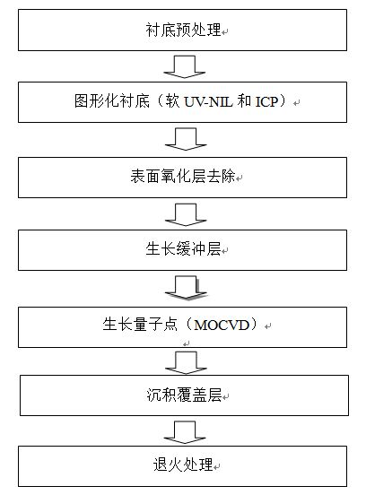
[0054] The technical route of self-organized growth of highly uniform and ordered quantum dot arrays based on soft UV-NIL and MOCVD can be found in figure 1 , including: ①substrate pretreatment; ②patterned substrate; ③remove surface oxide layer; ④grow buffer layer; ⑤grow quantum dots;

[0055] Figure 2a-Figure 2g It is a schematic diagram of making the quantum dot array of the present invention.

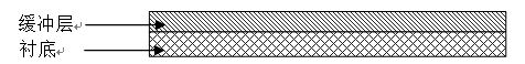
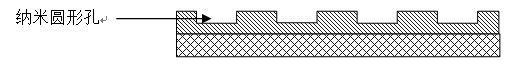
[0056] Its basic technological process is: (a) Figure 2a In, after the substrate is cleaned and decontaminated, a buffer layer with a thickness of 100-200nm is grown on it; (b) Figure 2b Among them, a large-area nanohole pattern array was fabricated on the substrate by soft UV-NIL and inductively coupled plasma etching (ICP); (c) Figure 2c In, use the oxide layer removal process to remove the oxide layer on the graphic surface; (d) Figure 2d In, a buffer layer of 10-30nm was grown; (e) Figure 2e In, MOCVD is used to grow highly uniform and orderly quantum dot arrays with c...


PUM

PropertyMeasurementUnit
diameteraaaaaaaaaa
depthaaaaaaaaaa
diameteraaaaaaaaaa

Abstract

The invention relates to a manufacture method of a large-area highly uniform sequential quantum dot array. The method comprises the following steps of: preparing a nanopore graphic array on a substrate by adopting soft ultraviolet nano imprint lithography (UV-NIL) and an inductively coupled plasma (ICP) technology; and growing quantum dots in a self-organizing way by using a prepared graphical substrate as a template and using a metal organic chemical vapor deposition (MOCVD) system. The invention realizes the low-cost, consistent and batched preparation of the large-area highly uniform sequential quantum dot array and can be applied to manufacture of devices such as quantum dot lasers, quantum dot memories, quantum dot solar batteries, quantum dot LEDs, single photon emitters, and the like.

Description

technical field [0001] The invention belongs to a method for manufacturing a semiconductor quantum dot array in the technical field of preparation and application of nanomaterials and structures, and in particular relates to a method for manufacturing a self-organized, highly uniform and ordered quantum dot array with a controllable position and a large area. It belongs to the technical field of preparation and application of nanometer materials and structures. Background technique [0002] Semiconductor nanostructures represented by semiconductor quantum dots (Quantumdot, QD) have very broad application prospects in the fields of optoelectronics, nanoelectronics, and quantum devices. The production of quantum dots and their quantum dots with uniform size, spatial order, and position control Arrays (Quantumdotarrays, QDAs) are used to realize many high-performance quantum dot devices (such as quantum dot lasers, quantum dot memories, quantum dot solar cells, quantum dot LEDs...

Claims


Application Information

Patent Timeline
Patent Type & Authority Applications(China)
IPC IPC(8): B82B3/00
Inventor 兰红波楼刚波尔.伍都宾贝格.笛特丁玉成
Owner SHANDONG UNIV
Why Eureka
Try Eureka