Apparatus and method for graphically producing nano structures by way of electrode induction and microwave curing

A nanostructure, microwave curing technology, applied in the fields of nanostructure manufacturing, nanotechnology, nanotechnology, etc., can solve the problems of many defects, low nanoimprint mold life, difficult to align, etc., to achieve high productivity, simple structure, graphics high precision effect

Inactive Publication Date: 2010-09-22
SHANDONG UNIV
View PDF3 Cites 11 Cited by
  • Summary
  • Abstract
  • Description
  • Claims
  • Application Information

AI Technical Summary

Problems solved by technology

[0003] Aiming at the problems of low service life, many defects and difficult alignment of nanoimprinting molds in the prior art, the present invention discloses a device and method for fabricating nanostructures on thermosetting epoxy resin materials using patterned electrode induction and microwave curing

Method used


Image

  • Apparatus and method for graphically producing nano structures by way of electrode induction and microwave curing
  • Apparatus and method for graphically producing nano structures by way of electrode induction and microwave curing
  • Apparatus and method for graphically producing nano structures by way of electrode induction and microwave curing

Examples


Embodiment Construction

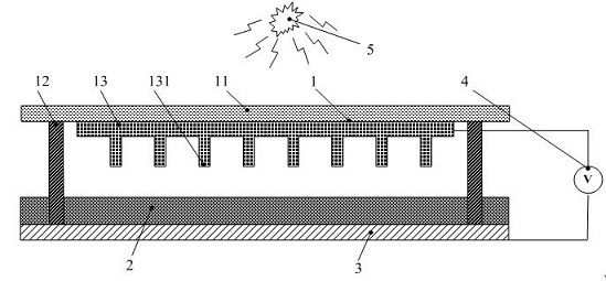
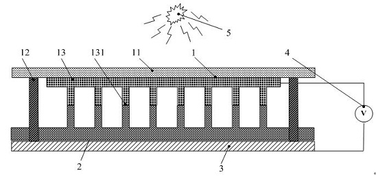
[0047] The schematic diagram of the nanostructure device produced by patterned electrode induction and microwave solidification disclosed by the present invention is as follows Figure 1a , Figure 1b shown. It consists of five parts: forming system 1, forming material 2, substrate 3, DC electric field 4, and microwave curing system 5. The forming system 1 is composed of a back plate 11 , a support 12 and a patterned electrode 13 . The back plate 11 plays the role of support and connection. The support 12 and the patterned electrode 13 are assembled into a complete forming system through the back plate 11. The function of the support 12 is to maintain a uniform gap between the patterned electrode 13 and the substrate 3 , the height difference between the support 12 and the nanostructure-inducing protrusion 131 (characteristic pattern to be transferred) formed by the protruding part of the patterned electrode determines the height of the fabricated nanostructure. Therefore, b...


PUM

PropertyMeasurementUnit
heightaaaaaaaaaa
thicknessaaaaaaaaaa

Abstract

The invention relates to an apparatus and a method for graphically producing nano structures by way of electrode induction and microwave curing. The apparatus comprises a molding system, a molding material, a substrate, a nano structure induction system and a microwave curing system. The method for producing nano structures based on the apparatus includes the following steps: (1) the fabrication of the molding system; (2) the preprocessing of the substrate; (3) the coating of the molding material; (4) the positioning of the molding system; (5) the inductive production of a nano structure; (6)the microwave curing of the nano structure; and (7) demolding. The invention is characterized by simple structure, low cost, high productivity, long electrode service life, high pattern precision andthe like, and can efficiently produce nano structures less than 100 nanometers at low cost.

Description

technical field [0001] The invention belongs to the technical field of microfabrication, and relates to a device and method for producing nanostructures by patterned electrode induction and microwave solidification. Background technique [0002] The microfabrication of nanostructures or patterns is the basis for the fabrication of nanoelectronics and nanodevices. At present, there are many methods for fabricating nanostructures, mainly including extreme ultraviolet lithography EUVL, electron beam direct writing lithography, ion beam projection lithography, X Radiation lithography, scanning probe microfabrication, molecular self-assembly, dip pen lithography, microcontact printing, nanoimprint lithography, etc. However, these techniques are usually complex, inefficient, and expensive. For example, although electron beam direct writing lithography has very high precision, the production efficiency is very low. Although nanoimprint lithography (NIL) has the characteristics of...

Claims


Application Information

Patent Timeline
Patent Type & Authority Applications(China)
IPC IPC(8): B82B3/00
Inventor 兰红波丁玉成
Owner SHANDONG UNIV
Why Eureka
Try Eureka