

Preparation method of low-resistance p-GaN ohmic contact electrode
A technology of ohmic contact electrodes and transparent electrode layers, which is applied in the manufacture of circuits, electrical components, and final products, can solve the problems of solvent volatilization or precipitation, inconvenient and effective control of process conditions, and poor process repeatability, etc., to achieve simplified operation, The effect of reducing the possibility of process fluctuations and simplifying operation requirements
- Summary
- Abstract
- Description
- Claims
- Application Information
AI Technical Summary
Problems solved by technology
Method used
Image

Examples
Embodiment 1
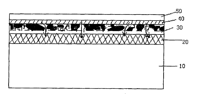
[0047] The removal of the oxide on the surface of the device epitaxial layer 20 in this example can be aimed at any metal electrode structure including Ni / Au electrode metal. In this example, a closed water bath device was used to prepare the required buffered HF treatment solution with a volume ratio of 2:1 between 1 mol / L ammonium bifluoride solution and 40% HF acid solution.
[0048] First, the epitaxial layer 20 of the GaN device is grown on the substrate 10 by MOCVD, and rapidly annealed at 750° C. for 15 minutes in nitrogen to activate carriers in the p-type layer. Then use trichlorethylene, acetone, methanol, ethanol, and deionized water to ultrasonically clean the epitaxial wafer for five minutes each, to remove organic pollutants adhered to the device epitaxial layer 20 during the growth process, and rinse with sufficient deionized water and blow dry with nitrogen. After completing other process steps of device preparation (depending on the specific device), photolit...
Embodiment 2
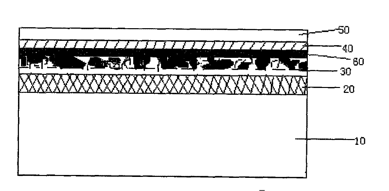
[0052] The removal of the high-resistance layer 60 in this example is mainly aimed at electrode structures such as Ni / Au, and the closed water bath device is still used, and the solution used is an oxalic acid solution with a mass fraction of 10%.
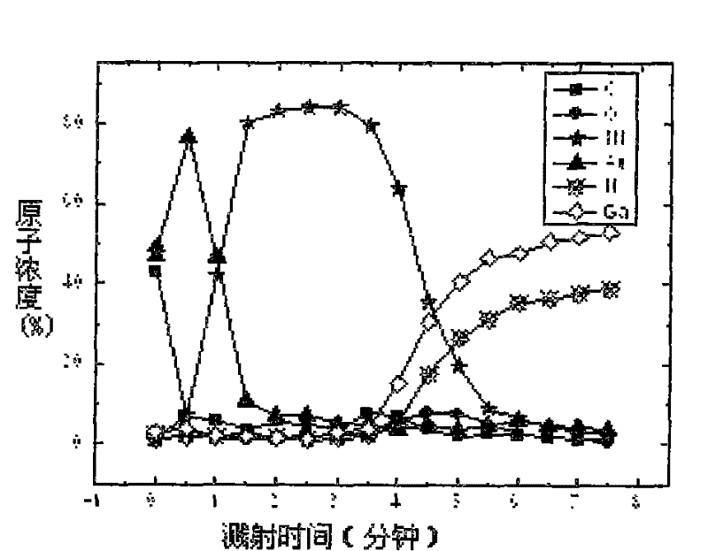
[0053] The specific operation steps are: remove the oxide on the epitaxial layer of the device according to Example 1 and deposit the epitaxial wafer with a Ni / Au=5nm / 5nm metal structure after electrode stripping, preferably annealing in oxygen at 550°C for 10 minutes, annealing The morphology and distribution of elements on the surface of the front and rear electrodes can be found in image 3 and Figure 4 The AES spectrum shown. Adjust the temperature of the water bath device to 70°C, and after it stabilizes, use the same method as in Example 1 to place the annealed epitaxial wafer in a polytetrafluoroethylene basket and put it into the 10% oxalic acid solution beaker, rinse the epiwafer with copious amounts of deionized water ...
PUM
 Abstract
Description
Claims
Application Information