Silicon dioxide optical waveguide device based on B-Ge-codoped upper cladding and preparation method thereof

A technology of silicon dioxide and optical waveguide, which is applied in the direction of light guide, optical components, optics, etc., can solve the problems that phosphorus is easy to be affected by moisture, increase the process risk and product instability, and achieve the elimination of voids, reduce process cost and improve stability Effect

Active Publication Date: 2010-10-13
HANGZHOU LIGHTIP TECH CO LTD
View PDF9 Cites 13 Cited by
  • Summary
  • Abstract
  • Description
  • Claims
  • Application Information

AI Technical Summary

Problems solved by technology

However, this method additionally uses a highly toxic gas phosphine, and phosphorus is relatively easy to be affected by moisture, which increases the risk of the process and the instability of the product

Method used


Image

  • Silicon dioxide optical waveguide device based on B-Ge-codoped upper cladding and preparation method thereof
  • Silicon dioxide optical waveguide device based on B-Ge-codoped upper cladding and preparation method thereof
  • Silicon dioxide optical waveguide device based on B-Ge-codoped upper cladding and preparation method thereof

Examples


Embodiment Construction

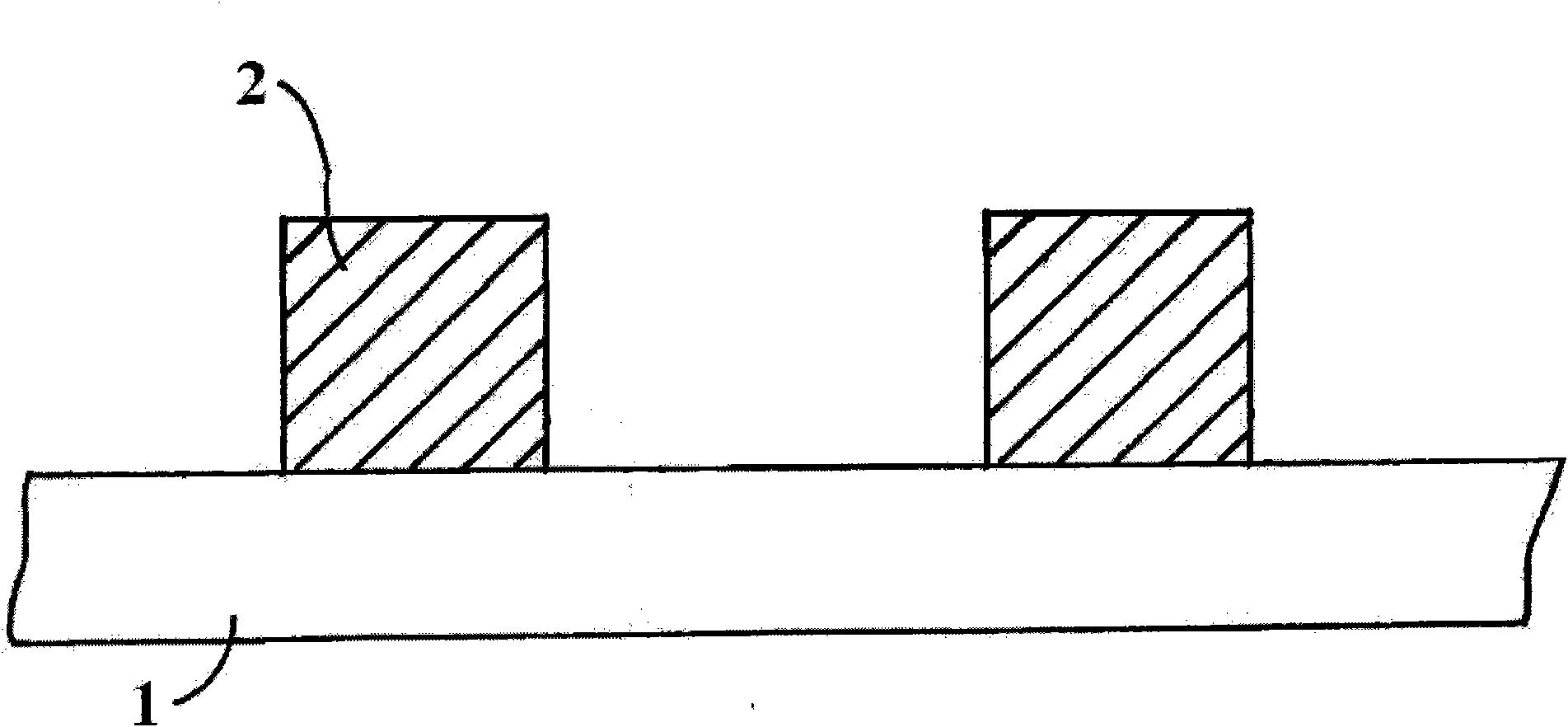
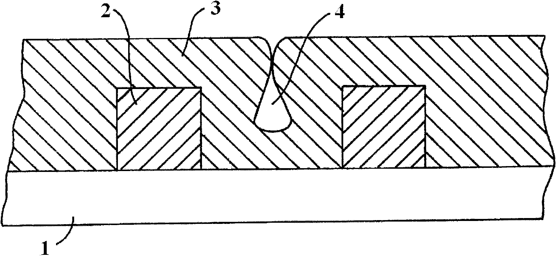
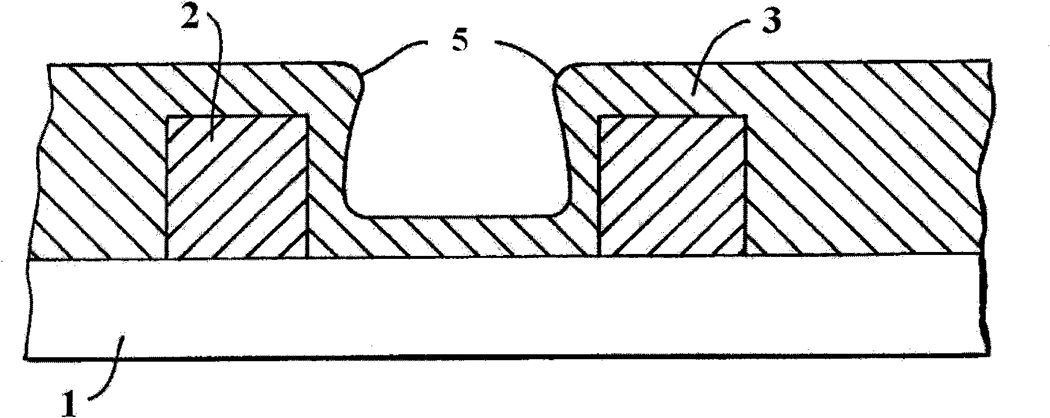
[0045] Such as Figure 5 As shown, in the present invention, a silicon dioxide lower cladding layer 1 is deposited on a substrate, and a germanium-doped silicon dioxide film is deposited on the upper surface of the lower cladding layer 1, and then a waveguide core layer 2 with a square section is formed by photolithography and etching processes. ; Deposit a layer of silicon dioxide upper cladding layer 3 doped with boron and germanium on top of the silicon dioxide lower cladding layer 1 and the waveguide core layer 2, and there is no gap between the upper cladding layer 3 and the core waveguide 2 structure .

[0046] The deposited silicon dioxide upper cladding layer 3 doped with boron and germanium has the same refractive index as the silicon dioxide lower cladding layer 1, and the melting point and refractive index of the silicon dioxide upper cladding layer 3 are lower than the waveguide core Layer 2.

[0047] The present invention describes a silicon dioxide optical waveguide...


PUM


Abstract

The invention discloses a silicon dioxide optical waveguide device based on a B-Ge-codoped upper cladding and a preparation method thereof. The preparation method comprises the following steps of: sedimentating a silicon dioxide lower cladding on a substrate, sedimentating a Ge-doped silicon dioxide film on the upper surface of the lower cladding, forming waveguide sandwich layers with a square cross section by lithography and etching processes; sedimentating a B-Ge-codoped silicon dioxide upper cladding on the silicon dioxide lower cladding and the waveguide sandwich layers without forming a gap between the upper cladding and the waveguide structure of the sandwich layer; and carrying out a high-temperature thermal-annealing process on the sedimented B-Ge-codoped silicon dioxide upper cladding and refluxing the upper cladding film with a low melting point into a gap between adjacent waveguide sandwich layers so that the shadowing effect action is lessened in a subsequent sedimentation film layer to fully fill the inter-waveguide gap and lessen the device loss. The silicon dioxide waveguide device structure based on the B-Ge-codoped upper cladding can be widely applied to devices in a waveguide structure with a high aspect ratio, such as splitters, couplers, array waveguide gratings, and the like.

Description

Technical field [0001] The invention relates to a planar optical waveguide device, in particular to a silicon dioxide optical waveguide device based on a boron-germanium co-doped upper cladding layer and a preparation method thereof. Background technique [0002] In the field of electronic technology, the development of discrete devices into integrated circuits has changed the production mode of the electronics industry. Similarly, in the field of optical technology, the current single form of various optical components on the road to integrated optics in the future will also greatly change the current status of traditional optical technology, and have a profound impact on the development of military and civilian information systems. Similar to the concept of IC chips, Planar Lightwave Circuits (PLCs) use manufacturing technology compatible with traditional semiconductor processes (Complementary Metal Oxide Semiconductor, CMOS) to integrate optical modules on the wafer, which hel...

Claims


Application Information

Patent Timeline
Patent Type & Authority Applications(China)
IPC IPC(8): G02B6/122G02B6/132
Inventor 何建军林旭峰
Owner HANGZHOU LIGHTIP TECH CO LTD
Why Eureka
Try Eureka