Method for manufacturing sloped sidewall silicon dioxide structure by adopting photoetching and dry etching

A technology of silicon dioxide and dry etching, which is applied in the field of semiconductor technology, can solve the problems of unsuitable MEMS devices, high equipment requirements, and easy breakage, etc., and achieve good electrical connection, strong universality, and the effect of avoiding breakage

Inactive Publication Date: 2010-10-20
INST OF SEMICONDUCTORS - CHINESE ACAD OF SCI
View PDF0 Cites 20 Cited by
  • Summary
  • Abstract
  • Description
  • Claims
  • Application Information

AI Technical Summary

Problems solved by technology

However, this method is complex in process, high in equipment requirements, and high in cost, and is not suitable for the preparation of MEMS devices.
If no special connection column is made, when the sacrificial layer is removed and the structure is released and suspended, due to the stress, the structure is prone to fracture at the corner of the support end, resulting in structural failure

Method used


Image

  • Method for manufacturing sloped sidewall silicon dioxide structure by adopting photoetching and dry etching
  • Method for manufacturing sloped sidewall silicon dioxide structure by adopting photoetching and dry etching
  • Method for manufacturing sloped sidewall silicon dioxide structure by adopting photoetching and dry etching

Examples


Embodiment Construction

[0032] In order to make the object, technical solution and advantages of the present invention clearer, the present invention will be described in further detail below in conjunction with specific embodiments and with reference to the accompanying drawings.

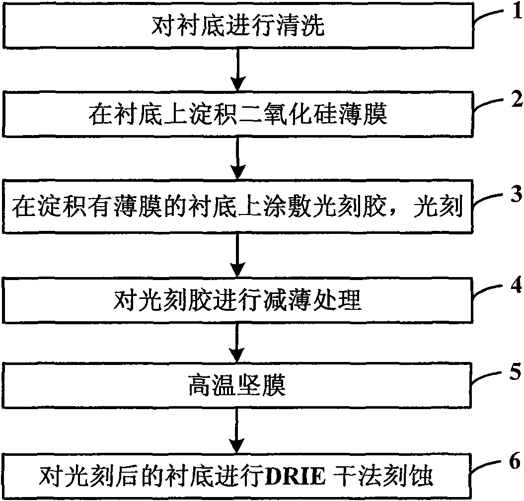
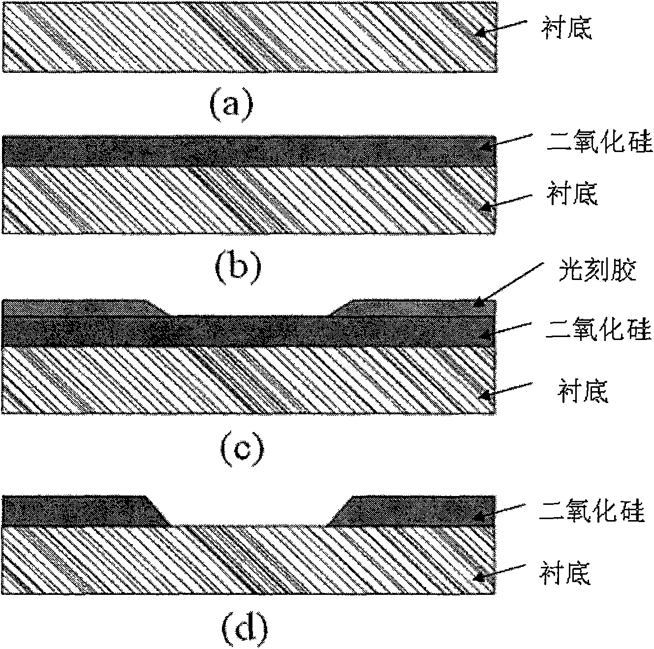
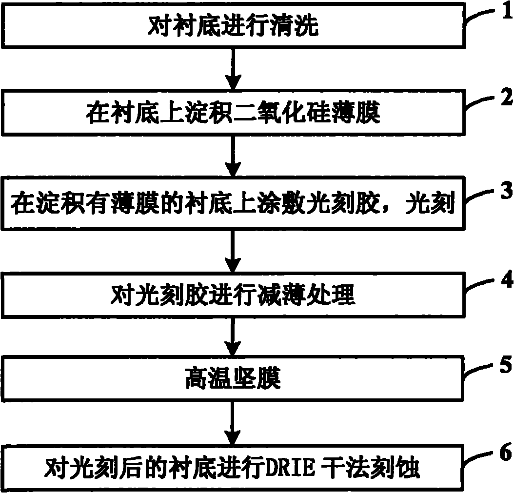
[0033] Such as figure 1 as shown, figure 1 It is a flow chart of a method for fabricating a silicon dioxide structure with inclined sidewalls by photolithography and dry etching provided by the present invention, and the method includes:

[0034] Step 1: cleaning the substrate;

[0035] For Si wafers or SOI wafers, the standard RCA cleaning process is used to clean the substrate; for quartz wafers, acetone, ethanol, and deionized water are used to clean the samples ultrasonically.

[0036] Step 2: Depositing a thin film on the substrate;

[0037] In this step, the substrate is placed in a plasma-enhanced chemical vapor deposition (PECVD) vacuum chamber and preheated for 5 minutes to raise the temperature of the substra...


PUM

PropertyMeasurementUnit
angleaaaaaaaaaa
angleaaaaaaaaaa

Abstract

The invention discloses a method for manufacturing a sloped sidewall silicon dioxide structure by adopting photoetching and dry etching. The method comprises the following steps of: (1) cleaning a substrate; (2) depositing a silicon dioxide thin film on the substrate; (3) coating photoresist on the substrate with the deposited thin film and photoetching; (4) thinning the photoresist; (5) hardening the film at high temperature; and (6) carrying out DRIE (Deep Reactive Ion Etching) dry etching on the photoetched substrate. A sloped silicon dioxide sidewall appearance can be obtained by photoetching and etching only once, and the method is simple and quick and has strong universality.

Description

technical field [0001] The invention relates to the field of semiconductor technology, in particular to a method for manufacturing a silicon dioxide structure with inclined side walls by photolithography and dry etching. Background technique [0002] Micro-Electro-Mechanical System (MEMS) refers to a micro-electro-mechanical system that integrates micro-sensors, micro-actuators, signal processing and control circuits, interface circuits, communication systems, and power supplies. It is a high-tech frontier discipline developed on the basis of microelectronics technology and integrated with various microfabrication technologies. Compared with traditional electromechanical systems, MEMS realizes the transformation between force, heat, magnetism, light and other signals and electrical signals on the chip, realizes the miniaturization, intelligence, and integration of information systems, improves performance, and reduces power consumption. Consumption and cost. [0003] Silic...

Claims


Application Information

Patent Timeline
Patent Type & Authority Applications(China)
IPC IPC(8): B81C1/00
Inventor 唐龙娟杨晋玲解婧李艳杨富华
Owner INST OF SEMICONDUCTORS - CHINESE ACAD OF SCI
Why Eureka
Try Eureka