Ingot casting method for quasi-monocrystalline silicon

A quasi-single crystal silicon and seed crystal technology, applied in the field of quasi-mono-silicon ingots, can solve the problems of being unsuitable for large-scale production, increasing the cost of ingots, complicated processes, etc., achieving easy operation, easy industrialization, and low cost. cost effect

Inactive Publication Date: 2010-10-20
晶海洋半导体材料(东海)有限公司 +1
View PDF7 Cites 72 Cited by
  • Summary
  • Abstract
  • Description
  • Claims
  • Application Information

AI Technical Summary

Problems solved by technology

The BP SOLAR company of the United States has done a lot of work around this topic. Its patent US2007/0169684A1 has reported a variety of methods, one of which is to place the seed crystal and the silicon material separately, and pour the molten silicon liquid into the layer covered with the seed crystal. The crystal growth is carried out in a container, because the two contain

Method used


Image

  • Ingot casting method for quasi-monocrystalline silicon
  • Ingot casting method for quasi-monocrystalline silicon
  • Ingot casting method for quasi-monocrystalline silicon

Examples


Embodiment 1

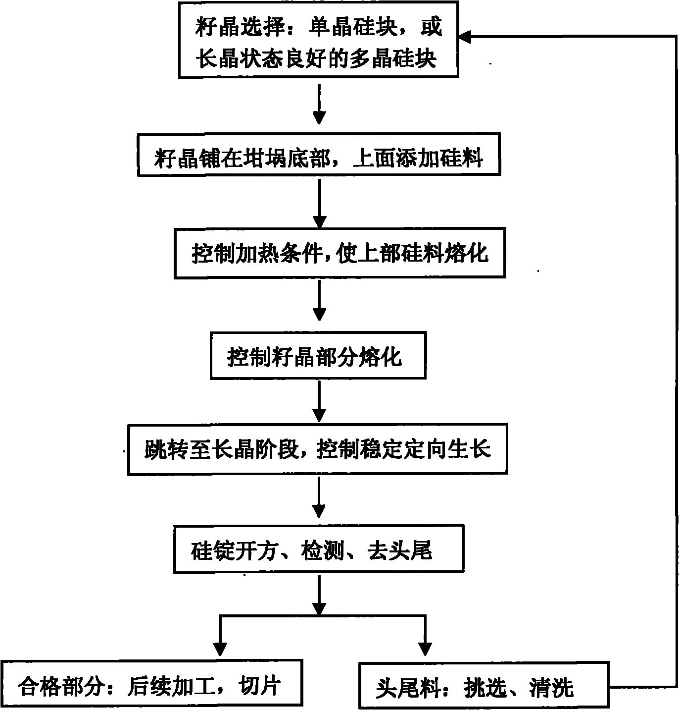
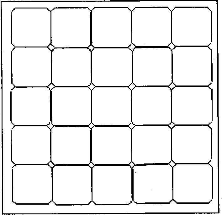
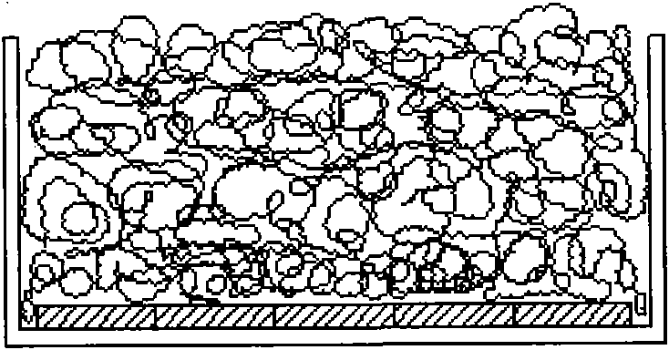
[0029] The (100) oriented single crystal rod obtained by the Czochralski method was squared to obtain a square column with a cross-sectional size of 156×156 mm, which was cut into 40-50 mm thick blocks as seed crystals. Choose a standard 450kg quartz crucible, that is, the internal size is 840×840×400mm, select 25 pieces of 156×156mm seed crystals according to the above standards, and spread them tightly on the bottom of the crucible in a 5×5 manner, and try to center the seed crystals when placing them. That is, the distance between the most edge surface of the peripheral seed crystal and the inner wall of the crucible is similar. The primary polycrystal is placed on top of the seed crystal, and a total of 430kg is loaded including the seed crystal. The specific arrangement of the seed crystal and the filling method of the seed crystal, silicon material and dopant are shown in the attached Figure 2a , 2b As shown, the dopant is boron, gallium or phosphorus, and the resistiv...

Embodiment 2

[0033] Square the (100) crystal orientation single crystal rod obtained by the Czochralski method to obtain a silicon rod with a cross-sectional size of 156×156mm and a length of about 160mm and 310mm, and then cut it along the radial direction to obtain a silicon rod with a size of 156×310×30mm , 156*160*30mm seed crystal. According to each row of 2 pieces of 310mm and 1 piece of monocrystalline silicon block of 160mm, they are closely arranged with a side of 156mm, and a total of 15 seed crystals are tiled in 5 rows in a quartz crucible of 840×840×400mm, and the seeds are placed as far as possible. The crystal is in the middle, that is, the edge surface of the peripheral seed crystal is close to the inner wall of the crucible. The primary polycrystal is placed on top of the seed crystal, and a total of 430kg is loaded including the seed crystal, and the target resistivity of doping is 1.5Ω.cm.

[0034] Vacuum after loading, control the power to heat to 1000-1400°C; after en...

Embodiment 3

[0037] As in Example 1, 13 (100) single-crystal seed crystals were obtained; in addition, the silicon ingots obtained by casting quasi-single-crystal silicon ingots were squared, detected, and cut with a band saw, and the cut bottom silicon blocks ( Mainly the remaining seed crystal) and the top large-grained silicon block are selected and processed, and the upper and lower impurity-enriched layers are removed and then cleaned, which is used as another part of the seed crystal. In this example, 6 remaining seed crystal silicon blocks recovered at the bottom and 6 large-grained silicon blocks at the top were each used as seed crystals, with a thickness of 2.5 to 3 cm. The 25 seed crystals obtained above were closely arranged in a 5×5 pattern and laid flat in a standard quartz crucible with an internal size of 840×840×400 mm, and were arranged in a symmetrical manner for different types of seed crystals for effect comparison. A total of 430kg of material is charged including the...


PUM


Abstract

The invention relates to an ingot casting method for quasi-monocrystalline silicon, which comprises the following steps of: (1) laying seed crystals at the bottom of a quartz crucible and adding a silicon material and a doping agent on the seed crystals; (2) vacuumizing and heating the crucible with the materials, raising the temperature in sections to melt the silicon material on the upper part, when the seed crystals begin to melt at the later stage of melting, controlling the temperatures and heating rates of a heater and the bottom of the crucible to partially melt the seed crystals and then entering a crystal growing stage; (3) cooling the heater in sections at the stage of crystal growing to make silicon crystals grow along the direction of unmelted seed crystals, and annealing and cooling after the silicon crystals grows to obtain large-gain silicon ingots; and (4) performing subsequent treatment on the large-grain silicon ingots to obtain the quasi-monocrystalline silicon. In the method, melting and crystal growing and the like are finished in the same equipment and in the same crucible, and the seed crystals are melted by controlling the temperature of the bottom of the crucible and the heating rate of the heater, so that the method has the advantages of low cost, easy operation and suitability for mass production; and the prepared quasi-monocrystalline silicon has high conversion efficiency, and the seed crystals can be recycled.

Description

technical field [0001] The invention belongs to the field of solar cells, and in particular relates to a method for ingot casting of quasi-single silicon. Background technique [0002] In the rapidly developing photovoltaic industry, high efficiency and low cost have always been the two main points of competition. As the most important solar cell material at present, crystalline silicon has always occupied an absolute advantage by virtue of its high efficiency and stability. [0003] Monocrystalline silicon is generally produced by the Czochralski method (CZ method). A single crystal seed crystal with a specific crystal orientation is used for seeding, and a single crystal silicon rod with the target crystal orientation is obtained after rotation and pulling. The resulting product contains only one crystal grain. It has the characteristics of low defects and high conversion efficiency, especially the wide application of alkali texturing method makes monocrystalline silicon c...

Claims


Application Information

Patent Timeline
IPC IPC(8): C30B29/06C30B28/06C30B33/02
Inventor 黄新明钟根香赵波徐芳华
Owner 晶海洋半导体材料(东海)有限公司
Why Eureka
Try Eureka