Micro-fluidic chip for micro-magnetic field control and manufacturing method thereof

A technology of microfluidic and microfluidic devices, applied in the field of microfluidic chips controlled by micromagnetic fields and its production, can solve the problems of difficult observation and high requirements for instruments and equipment, and achieve the effect of avoiding direct contact

Inactive Publication Date: 2010-11-10
WUHAN UNIV
View PDF1 Cites 21 Cited by
  • Summary
  • Abstract
  • Description
  • Claims
  • Application Information

AI Technical Summary

Problems solved by technology

Others use electron beam physical vapor deposition of a micropattern of titanium on the photoetched substrate, and then deposit a few hundred nanometers of nickel on it, and finally use plasma-enhanced chemical vapor deposition of a layer of silicon dioxide to coat the nickel. The mi

Method used


Image

  • Micro-fluidic chip for micro-magnetic field control and manufacturing method thereof
  • Micro-fluidic chip for micro-magnetic field control and manufacturing method thereof
  • Micro-fluidic chip for micro-magnetic field control and manufacturing method thereof

Examples


Embodiment Construction

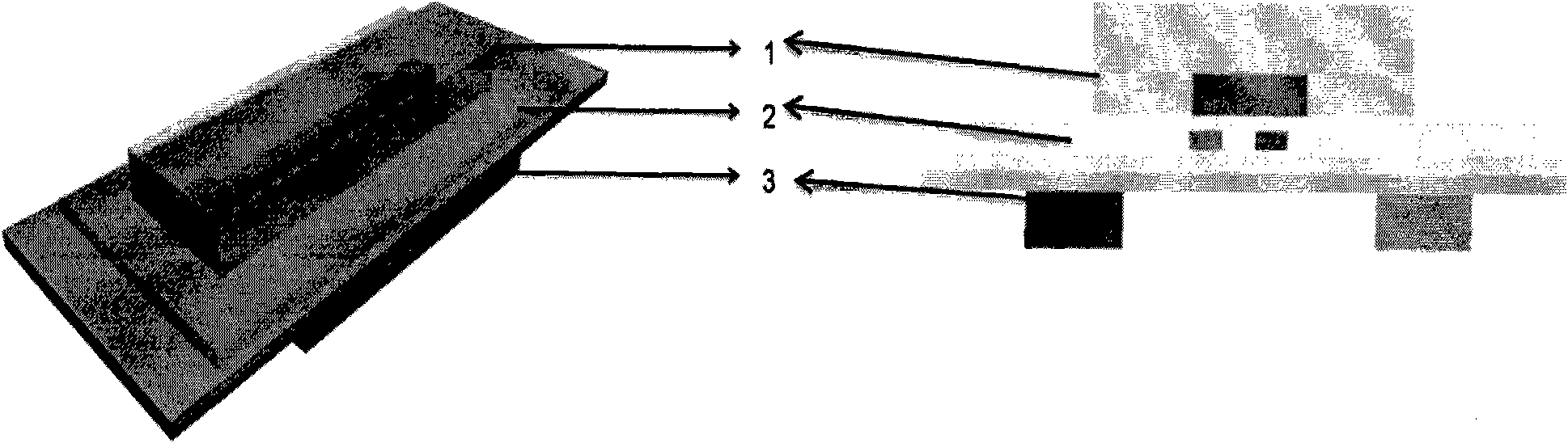
[0031] 1. Production:

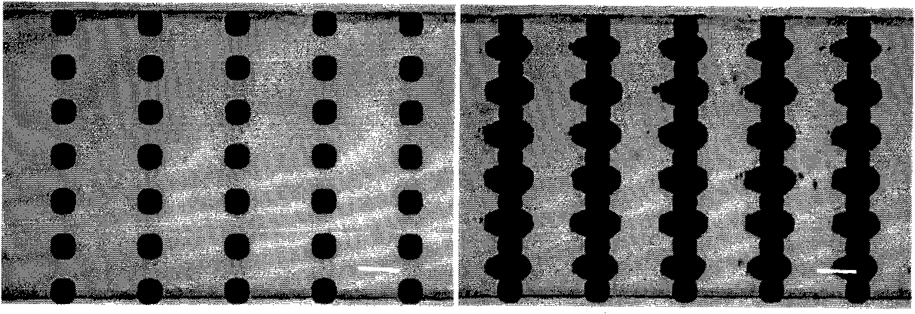
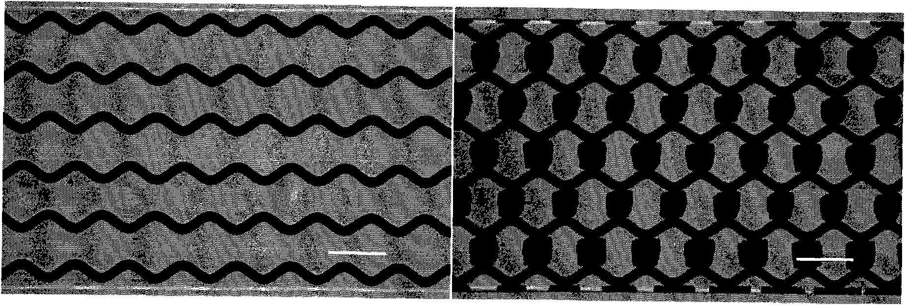
[0032] (1) Cut the ITO conductive glass into a size of 30mm x 80mm, ultrasonically clean it in ethanol and ultrapure water, and then apply a layer of AZ4620 photoresist with a height of about 12 μm, pass through a printed mask, UV exposure is carried out under the machine to form the same pattern as on the mask. Then, in the electroplating bath, using a DC power supply and a large piece of nickel, electroplating is performed, and then the photoresist is removed in acetone, so that a tiny pattern of nickel is formed on the ITO conductive glass. Then adjust a polydimethylsiloxane (PDMS) prepolymer with a mass ratio of 15:1 (RTV615A:B), remove air bubbles in a vacuum, and use a plastic throwing machine to throw out a polydimethylsiloxane (PDMS) prepolymer of about The PDMS layer with a thickness of 8 μm was cured in an oven for half an hour. This encapsulates the nickel micropatterns in PDMS, avoids contact with magnetic beads in subsequent experiments, ...


PUM


Abstract

The invention discloses a micro-fluidic device for micro-magnetic field control and a manufacturing method thereof. The device consists of a micro-fluidic fluid layer chip, a substrate provided with soft magnetic material micro-patterns, and a magnetic source body. The substrate provided with the soft magnetic material micro-patterns is a transparent conducting substrate, wherein the micro-patterns are arranged and designed corresponding to needed magnetic beads, and a layer of a polymeric material is covered on the micro-patterns to realize a connection in a permanent irreversible bonding mode with the micro-fluidic fluid layer chip. Under the action of an external magnetic field, nickel micro-patterns are magnetized and generate a strong local magnetic field gradient to realize the magnetic field control in a micron range. The device can capture magnetic substances at a high flow speed, and can release the magnetic substances at a low flow speed after the magnetic source body is removed. The device can be used in the fields of organism-targeted material detection, gene analysis, quick immunoassay, cell screening and the like.

Description

technical field [0001] The invention belongs to the technical field of microfluidic chips. In particular, it relates to a microfluidic chip controlled by a micromagnetic field and a manufacturing method thereof. Background technique [0002] Microfluidic chip technology was developed in the field of analytical chemistry in the 1990s. It builds a chemical or biological laboratory on a chip of a few square centimeters, and processes and reacts various samples involved in chemical and biological experiments. , separation, detection, etc. are integrated together to complete various functions under the routine biochemical laboratory. [0003] At the same time, as a solid-phase carrier, magnetic particles have a wide range of applications in the identification, separation, control of drug delivery, and cell sorting of targeted substances. Combining magnetic bead technology on microfluidic chips is one of the hot issues in current research. Due to scale limitations (generally pe...

Claims


Application Information

Patent Timeline
IPC IPC(8): B01L3/00B01J19/00G01N35/00
Inventor 张志凌余旭庞代文
Owner WUHAN UNIV
Why Eureka
Try Eureka